
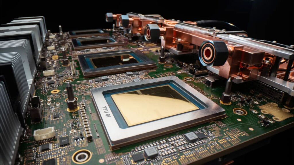
Samsung Foundry is reportedly considering outsourcing part of the physical design of the input and output chip of Google’s upcoming AI accelerator, known internally as Icefish. This move would allow the component to be adapted to Samsung’s fabrication facilities, while TSMC would handle the main compute chiplet. However, neither company has confirmed the final distribution of responsibilities yet.
The key points of Google’s next TPU in 20 seconds
- Google might split Icefish among several manufacturers and design partners.
- TSMC would produce the main AI compute chiplet.
- Samsung would take on a component for input, output, and memory interface.
- Several South Korean companies are competing for Samsung’s physical design contract.
- Reports vary regarding the manufacturing processes and final packaging.
This information comes from South Korean media and expands on an earlier report suggesting Google was negotiating with Samsung for manufacturing part of its upcoming Tensor Processing Unit (TPU). That initial report estimated mass production could start around 2028, with Samsung’s part using a 2-nanometer process. Reuters has not been able to independently verify these discussions.
The new report mentions three potential contractors: ADTechnology, Gaonchips, and Alphachips. Samsung would entrust them with the so-called back-end design, which involves converting a logical architecture into a physical layout suitable for fabrication. This phase should not be confused with final assembly or chip packaging.
In this context, it refers to transforming an architectural design into a physical layout—including placement of blocks, routing of millions of connections, power and clock distribution, thermal analysis, timing verification, and meeting process design rules of Samsung’s manufacturing nodes.
How the Icefish future TPU would be divided
The most advanced AI accelerators are no longer necessarily built as a single piece of silicon. They can be divided into specialized chiplets assembled within a single package.
The compute chiplet contains matrices and units that perform operations used by AI models. The input/output component handles data movement between this core, high-bandwidth memory, other accelerators, and the hosting system.
| Participant | Assigned role in Icefish | Current status |
|---|---|---|
| TPU architecture and system design | Confirmed as the TPU family designer | |
| MediaTek | Collaboration on ASIC design | Reported by various sources; not confirmed by MediaTek |
| TSMC | Production of the main compute chiplet | Widely supported by information |
| Samsung Foundry | Manufacturing of input/output or memory interface chip | In negotiations; no official confirmation |
| ADTechnology | Possible physical design for Samsung process | Cited by South Korean media |
| Gaonchips | Possible physical design for Samsung process | Cited by South Korean media |
| Alphachips | Possible physical design for Samsung process | Cited by South Korean media |
| TSMC or Intel | Possible advanced packaging technologies | Contradictory information exists about these options |
Engaging a design house wouldn’t mean Samsung has abandoned the order. The foundry would still produce the silicon but would work with a specialized partner to finalize the physical implementation and ensure compliance with manufacturing rules.
This approach is common with application-specific integrated circuits (ASICs), where the client defines architecture and functions; a specialized firm converts this into a verifiable design, and the foundry manufactures the wafers.
For Samsung, outsourcing part of the work also allows resource allocation at a time when its foundry business is attempting to take on more advanced orders. The report attributes this decision to the workload the company is experiencing, though no volume targets, signed contracts, or deadlines are provided.
Discrepancies around TSMC, Samsung, and Intel
Icefish’s industrial roadmap is still uncertain. While various recent reports agree that Google plans to split the chip among multiple partners, details differ regarding manufacturing processes, Samsung’s involvement, and packaging strategies.
| Published info | Compute chiplet | I/O or memory chip | Packaging |
| Latest South Korean report | TSMC A14 | Samsung, with externalized physical design | Not finalized |
| The Information, via Reuters | TSMC, process details not specified | Samsung SF2 of 2 nm | Not finalized |
| JPMorgan estimates | TSMC N2 | TSMC N3 | Likely TSMC remains the main supplier |
| Intel-related info | Not necessarily manufacturing chiplets | Not confirmed | Google may consider EMIB or EMIB-T packaging |
| MediaTek statements | Tests with TSMC A14 | Does not identify Google as a client | Supports both CoWoS and EMIB |
The difference between A14 and N2 processes is significant. TSMC considers A14 as a generation beyond its 2nm process and expects volume production in 2028. MediaTek has confirmed working with various test chips based on A14 but has not publicly identified Google as a customer.
In June, a different configuration was suggested: TSMC would produce the main block, while Samsung would fabricate the component connecting the accelerator to memory using its 2nm process. Icefish was still under development, with mass production potentially beginning in 2028.
There are also questions regarding Intel. Some reports indicate discussions about using Intel’s advanced EMIB-T packaging in future custom chips for Google. MediaTek has said it can work with both TSMC’s CoWoS and Intel’s EMIB but declined to confirm whether Google plans to use either option.
Therefore, it’s still uncertain whether Samsung has sealed a definitive contract or if TSMC plans to use A14 for the compute chiplet. Google might be exploring various configurations or different project phases.
The design of this level of accelerator can evolve before entering mass production. Factors such as node performance, available capacity, wafer costs, packaging results, and memory availability could influence the final configuration.
Why Google wants to distribute manufacturing
TPUs have become a central part of Google’s infrastructure. The company uses them for training and deploying models, offering capacity on Google Cloud, and reducing reliance on Nvidia GPUs.
A technical paper published by Google researchers covering generations from TPU v2 through Ironwood illustrates the scale of progress. Over eight years, per-node memory capacity and bandwidth increased tenfold, maximum per-node performance rose a hundredfold, and overall supercomputing performance grew approximately 3,600 times.
This evolution demands more advanced silicon, larger memory, and bigger packaging. Relying on a single foundry for all components could become a bottleneck as demand for AI chips exceeds TSMC’s production capacity.
Dividing the project offers several potential benefits:
| Google’s goal | Possible advantage |
| Reduce dependency on TSMC | Access additional capacity at Samsung |
| Separate compute and interfaces | Choose optimal nodes for each component |
| Increase TPU production | Prevent a single process from limiting total orders |
| Compare foundries | Strengthen negotiation position |
| Diversify packaging options | Keep CoWoS and EMIB options open |
| Accelerate new generations | Work in parallel with multiple partners |
Not all components require the most advanced node. The compute chiplet benefits from high density and low power per operation, while the I/O component can prioritize reliable interfaces, memory controllers, and high-speed connections.
Manufacturing chiplets across different foundries adds complexity. Coordinating libraries, voltages, tolerances, packaging, signals, and testing is challenging, and deviations could impact performance or delay the entire accelerator.
For Samsung, obtaining the Icefish component would be valuable beyond initial volume. It would demonstrate that its 2nm process can participate in one of the most demanding AI accelerators on the market and could open doors for other custom chip designers.
The South Korean foundry also aims to strengthen its position versus TSMC in external markets. Google’s involvement would bring a notable workload, helping refine the node, boost fab utilization, and gain experience in high-bandwidth memory interface design.
Outsourcing physical design doesn’t necessarily diminish this value. It can also show that Samsung is building a local network of partners capable of taking projects from specifications to production.
Icefish appears to be moving toward a supply chain that is more distributed than previous generations. However, the picture remains incomplete: TSMC seems likely to handle the compute block, Samsung could be involved in memory and I/O, MediaTek is participating in design, and Intel is attempting to enter through packaging strategies.
Until Google or its partners confirm contracts, processes, and timelines, this project should be regarded as an ongoing industry negotiation, not as a finalized split of responsibilities.
Frequently Asked Questions
What part of Google’s TPU would Samsung manufacture?
Current reports suggest Samsung will handle the input/output or memory interface chip. Its final design and exact component name have not been officially confirmed.
Why would Samsung outsource the physical design?
Samsung might work with a specialized firm to adapt the chip for its process, complete placement and routing, and conduct final verification checks.
Will TSMC continue fabricating Google’s TPUs?
Most indications point to TSMC keeping the main compute chiplet. However, reports differ on whether it will use N2 or A14 processes, and whether it will also produce the I/O component.
What role could Intel play?
Intel’s involvement is unconfirmed. Known information links it mainly to its advanced EMIB or EMIB-T packaging technologies.
Sources:
- ETNews, regarding potential outsourcing of Icefish’s I/O component physical design.
