
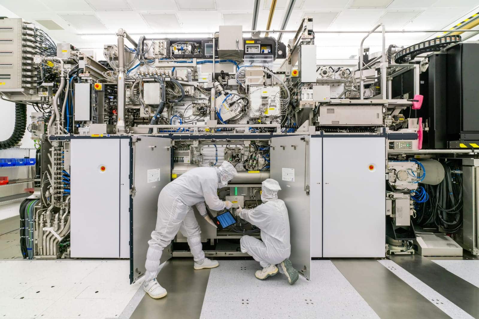
NVIDIA designs the accelerators that train large artificial intelligence models. TSMC turns those designs into chips. Apple, AMD, Intel, Samsung, and SK Hynix compete to manufacture increasingly smaller and more efficient processors and memories. But before any of them can produce them, they need machinery capable of transferring tiny circuits onto a silicon wafer with unprecedented precision.
Much of this technology comes from Veldhoven, a Dutch town where ASML is headquartered. The company doesn’t manufacture chips, develop AI models, or have direct consumer relations. Nonetheless, it is the sole commercial provider of extreme ultraviolet (EUV) lithography systems used to produce the most advanced semiconductors. David Bonilla described it in the Bonilista as “the company printing the future.” This phrase resonates because, before this future can run in data centers, it must be etched onto silicon.
ASML: Key Points in 20 Seconds
- ASML is a Dutch company founded in 1984 by Philips and ASM International.
- It manufactures lithography systems that project circuit patterns onto silicon wafers.
- It is the only commercial supplier of EUV machines for advanced chip production.
- TSMC, Samsung, Intel, SK Hynix, and other major manufacturers rely on its equipment.
- In 2025, it generated €32.7 billion in revenue and €9.6 billion in net profit.
- In Q1 2026, it reported €8.8 billion in sales, €2.76 billion in profit, and a gross margin of 53%.
- Revenue projections for 2026 range between €36 billion and €40 billion.
- Its order backlog at year-end 2025 was approximately €38.8 billion.
- Next-generation High-NA EUV systems can cost close to $400 million per unit.
- The main risk isn’t technological but stems from investment cycles, export controls, and geopolitical tensions among the U.S., China, and Europe.
ASML occupies a unique position. It doesn’t sell the product that the public recognizes, but it supplies one of the most critical tools without which that product cannot be manufactured. A NVIDIA processor may take center stage commercially, and TSMC can handle its production, but the capability to place billions of transistors depends on successive lithography stages.
The company also produces deep ultraviolet (DUV) lithography systems, which remain essential for many semiconductor layers and less advanced nodes. EUV has not replaced all previous lithography methods. It’s used where its shorter wavelength allows creating smaller patterns or reducing the number of exposures needed.
Recent ASML Results
| Indicator | 2025 | Q1 2026 |
|---|---|---|
| Revenue | €32.7 billion | €8.8 billion |
| Net profit | €9.6 billion | €2.76 billion |
| Gross margin | — | 53% |
| EPS | — | €7.15 |
| Order backlog | €38.8 billion | — |
| 2026 sales forecast | — | €36–40 billion |
These figures indicate a company with unusual margins for an industrial manufacturer and a high level of visibility into some of its future activity. The order backlog at the end of 2025 was roughly equivalent to one year of projected 2026 sales, though orders can change, and revenue realization depends on manufacturing, delivery, and installation schedules.
How a Drop of Tin Becomes a Chip
Lithography can be seen as a highly sophisticated printing process. The manufacturer starts with a silicon wafer coated with a light-sensitive material. The machine projects the pattern corresponding to a circuit layer onto it. Subsequent physical and chemical processes then create transistors, connections, and structures.
This operation is repeated multiple times. A modern chip isn’t created with a single exposure but through successive layers that must be precisely aligned. Even a tiny error can reduce the performance of the entire wafer and increase the cost per functional unit.
In EUV lithography, ASML uses light with a wavelength of 13.5 nanometers. To generate this, the system fires laser pulses at microscopic tin droplets. The impact creates a plasma that emits extreme ultraviolet radiation. Current versions produce and hit tens of thousands of droplets per second, while ASML works on more powerful sources to boost productivity.
The process is complex because EUV light is absorbed by nearly everything, including air. It cannot travel through conventional glass lenses. The path must be maintained in vacuum and uses multilayer mirrors developed by ZEISS, whose surface requires extraordinary precision.
The collaboration with the German optical group dates back to the early days of ASML. The relationship became so vital that in 2016, the Dutch firm acquired a 24.9% stake in Carl Zeiss SMT for around €1 billion. ZEISS retains majority ownership, but both companies share a deep technological interdependence.
Along with the light source and mirrors, systems that move the wafer and mask, vibration controls, cooling, software for correction, and thousands of sensors are all crucial. The machine must operate for hours at high speed without losing alignment between exposures.
Therefore, ASML shouldn’t be seen merely as a machinery manufacturer. It acts as an integrator of an international network of specialists. It determines which expertise to control directly, coordinates components from numerous suppliers, and ensures the entire system functions within its clients’ fabs.
The next generation is called High-NA EUV. The initials stand for a higher numerical aperture, enabling the focus of smaller structures. ASML claims these systems can reduce certain feature sizes by up to 66% compared to previous EUV editions. Intel, Samsung, and SK Hynix have moved forward with adoption, while TSMC remains more cautious due to cost and the timeline for economic viability.
A High-NA unit can approach $400 million. The cost makes sense only if it eliminates additional exposures, improves performance, or enables processes that wouldn’t be feasible with older equipment. In semiconductors, the most expensive tool doesn’t always produce the most costly chip; instead, it can reduce steps and boost factory productivity.
From Challenging Project to Strategic Asset for Europe
ASML was born in 1984 as a joint venture between Philips and ASM International. Its early days were far from a story of a company destined to dominate global technology. It had few clients, needed substantial capital, and competed with Japanese firms like Nikon and Canon, which had more experience and a stronger market position.
The decisive decision was not to try to make everything in-house. ASML relied on specialized suppliers for key components and focused on design, integration, software, and relationships with chipmakers. Its modular approach also made it easier to repair and update equipment at customer sites.
The PAS 5500, introduced in the early 1990s, was pivotal in elevating the company’s profile. Over subsequent years, ASML closed the gap with competitors, becoming the leading provider of lithography systems by 2002. Transitioning to EUV involved decades of research, acquisitions, and collaborations with centers like imec and suppliers like ZEISS.
A 2012 event exemplifies its strategic evolution. Intel, TSMC, and Samsung—competitors among themselves—formed an investment consortium to accelerate EUV and other technology research. They acquired about 23% of ASML and provided additional funding for development. They paid for a problem that directly impacted their own industrial plans.
This created a rare dependency: ASML needed the chipmakers to continue investing in new fabs, and the chipmakers depended on ASML to turn EUV into an industrial reality. The relationship became mutually reinforcing.
That bond remains evident in 2026. SK Hynix announced the purchase of EUV equipment worth nearly $8 billion through 2027 to expand its HBM and DRAM memory production for AI applications. Reuters estimated the deal could include around 30 systems.
Demand driven by AI has fueled a new cycle of growth for ASML. Accelerators require advanced logic chips, high-bandwidth memory, interconnects, and additional manufacturing capabilities. The company earns not from individual inquiries but benefits as TSMC, Samsung, Intel, and SK Hynix build capacity to meet this demand.
Initially cautious, the company now considers AI a key driver for long-term growth. Yet, sector cyclicality remains—fab delays, investment adjustments, and excess capacity can occur when forecasts aren’t met.
Strengths and Risks of ASML
| Strengths | Why They Matter |
|---|---|
| Exclusive EUV supplier | Leading-edge chip manufacturers have no equivalent in production today |
| High technical barriers | Replicating the system requires mastery of light, optics, materials, vacuum, mechanics, software, and manufacturing |
| Close customer relationships | ASML anticipates parts of TSMC, Samsung, Intel, and memory chip plans years ahead |
| Strong order backlog | Helps smooth quarterly fluctuations and provides visibility |
| Revenue from service and upgrades | Machines require maintenance, spare parts, and upgrades over many years |
| Exposure to AI, logic, and memory markets | Demand isn’t limited to a single chip type |
| Risks | Potential Impacts |
|---|---|
| Semiconductor cycle | Downturns may delay orders, deliveries, and new fab investments |
| Limited client base | TSMC, Samsung, Intel, and memory makers represent much of the market |
| Export controls | Restrictions on China could limit sales of systems and services |
| Geopolitical pressures | ASML is caught between the strategic priorities of the U.S., China, and Europe |
| Supply chain complexity | A problem with a specialized supplier could delay entire systems |
| High-NA costs | Clients may delay adoption if advantages don’t justify the investment |
| High expectations | High stock valuation makes the company sensitive to forecast revisions |
China remains a key dilemma. While the country has been a major market for DUV equipment, U.S. and Dutch export controls on advanced technology have tightened. ASML doesn’t sell EUV machines to Chinese clients and requires licenses for certain less-advanced systems. New restrictions may also impact maintenance and updates for already-installed equipment.
This situation illustrates that ASML is a European company, but not entirely autonomous. It relies on technology, intellectual property, and components from the U.S., Germany, and other nations. Its main customers are in Taiwan, South Korea, and the U.S. Its strength stems from this international collaboration, which also exposes it to political decisions beyond the Netherlands.
One of Europe’s crucial lessons is that ASML didn’t emerge by copying Silicon Valley’s model or building a digital consumer platform. It was formed through applied engineering, manufacturing, German optics, European research, U.S. and Asian acquisitions, and even capital from its own clients.
While not a purely Dutch industrial firm, with its headquarters and decision centers in the Netherlands, it is the product of a network spanning Europe and connecting globally.
Europe often compares its technological weak points to giants like Google, Microsoft, Amazon, or NVIDIA. While that highlights gaps in software, cloud, and AI, it can obscure areas where Europe maintains capabilities hard to replicate. ASML is one such example.
Its history isn’t built on quick wins. The seemingly impregnable advantage took decades to develop. It involved years of uncertainty, collaboration with rivals, and funding technologies that might not have worked. It’s a form of industrial policy less visible than launching a new application but much harder to imitate.
ASML doesn’t build AI, nor can it claim sole credit for semiconductor advances. Without TSMC, Samsung, Intel, ZEISS, imec, and thousands of suppliers, its machines would have limited utility. Its significance lies in being the hub where all these capabilities converge.
This is why a largely unknown company to the general public has become one of the most watched by governments, manufacturers, and investors alike. ASML doesn’t control the entire future of chips, but it dominates one of the most irreplaceable tools for their manufacturing.
Analyzing its financials, strengths, and risks isn’t an investment recommendation. It’s a way to understand why the global race for AI began well before a GPU appeared in a data center.
Frequently Asked Questions
What exactly does ASML manufacture?
It produces photolithography systems used to project circuit patterns onto silicon wafers. It also develops software, metrology, and related services for those systems.
Why is ASML so crucial for NVIDIA?
NVIDIA designs its chips but relies on manufacturers like TSMC to produce them. TSMC uses ASML systems at various stages of its advanced process flows.
Does ASML hold a monopoly?
It’s the only commercial supplier of EUV systems used in advanced manufacturing. For DUV lithography, it competes with firms like Nikon and Canon.
Why are its machines so expensive?
They integrate EUV light sources, high-precision mirrors, vacuum systems, high-speed mechanics, sensors, and software. Next-generation High-NA systems can cost nearly $400 million each.
Sources:
- ASML’s financial results for 2025 and the first quarter of 2026.
- ZEISS, history of its collaboration, and ASML’s stake in Carl Zeiss SMT.
- David Bonilla, Bonilista 796, The company printing the future.
