
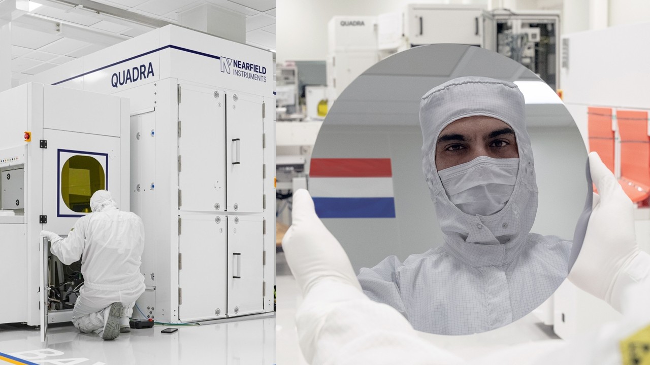
Artificial intelligence has spotlighted GPUs, data centers, and HBM memory, but there’s a less visible part of the semiconductor industry without which none of those advancements scale: metrology. Before manufacturing millions of advanced chips, tiny structures must be measured, defects detected, processes controlled, and the new generation’s production performance assured. This is the domain where Nearfield Instruments operates.
The Dutch company has closed a $380 million Series D funding round, the largest deep-tech funding round recorded in the Netherlands, according to the company itself. The operation values Nearfield Instruments at $1.6 billion and is led by Fidelity Management & Research Company, alongside Temasek, Walden Catalyst Ventures, Innovation Industries, M&G Investments, Invest-NL, and Qatar Investment Authority, in addition to existing investors like TNO Ventures and ING.
This figure is significant because it comes at a time when chip manufacturing is becoming more challenging, not easier. The transition to High-NA EUV, Gate-All-Around architectures, future CFET processes, stacked memory, HBM, hybrid bonding, and 3D integration requires more precise and faster inside-the-process measurements. Designing more complex chips isn’t enough; they must be manufacturable repeatedly.
Metrology becomes strategic
In semiconductors, metrology essentially means measuring what occurs inside a wafer during fabrication. Dimensions, shapes, roughness, alignments, defects, voids, feature depths, and layer uniformity. In advanced nodes and 3D packaging, these measurements are no longer final quality controls—they are integral to the industrial process itself.
Nearfield Instruments specializes in 3D metrology and inspection solutions for advanced manufacturing. Its product QUADRA employs a multi-head architecture with miniaturized AFMs to perform non-destructive, inline 3D measurements, applicable to VNAND, DRAM, HBM, advanced logic, high-aspect-ratio structures, EUV resist, and High-NA EUV, as well as hybrid bonding.
The company also offers AUDIRA, a subsurface, non-destructive metrology system designed to detect and measure buried features and defects, such as voids, in advanced memory and logic devices. This is especially relevant because in 3D architectures, many critical areas are not visible on the surface.
The value of these tools lies in accelerating time-to-yield. In a chip fab, even minor deviations can ruin very expensive wafers. If process control is delayed or lacks resolution, costs skyrocket. Proper, timely measurements enable early corrections, reduce waste, and stabilize production.
Why AI needs better measurements
The connection to AI might seem indirect, but it’s very clear. AI models demand more compute power, memory, bandwidth, and lower operational energy. Achieving this isn’t just about smaller transistors; it also relies on advanced packaging, vertical integration, direct chip-to-chip connections, HBM, and increasingly 3D architectures.
Each of these techniques introduces new manufacturing challenges. Hybrid bonding requires controlling surfaces, alignments, and bonds at extremely small scales. Gate-All-Around and CFET architectures increase the 3D complexity of transistors. High-NA EUV promises higher resolution lithography but also requires measuring more demanding patterns. HBM and stacked structures need internal defect control, as such issues can affect performance, heat, and reliability.
Nearfield claims its solutions enable accurate, reliable, high-performance measurements to control these processes and improve yield. While this is a commercial statement, it aligns with a well-known industrial reality: the more complex the chip, the more critical precise measurement during production becomes.
The funding will accelerate their innovation roadmap, help establish global application centers, expand manufacturing capacity, strengthen customer support, and deepen R&D collaborations with leading semiconductor manufacturers. This is key—having promising equipment isn’t enough; it must be installed, integrated into real fabs, maintained, and proven to improve high-volume processes.
Europe seeks greater influence in the chip supply chain
The funding round also has an European dimension. The Netherlands already holds a central position in the global semiconductor industry through ASML, but the ecosystem extends beyond lithography. Metrology, inspection, equipment, photonics, industrial software, and specialized suppliers form a chain where Europe retains important assets.
Nearfield Instruments emerged from this environment. TNO Ventures, one of its investors, describes Nearfield as a company focused on advanced metrologies for semiconductors, highlighting QUADRA as a nanometric-resolution 3D measurement system.
The entry of international investors like Fidelity, Temasek, or QIA also shows that metrology is no longer considered a secondary element. In an industry shaped by geopolitical tensions, export restrictions, and surging AI demand, controlling critical manufacturing tools can be as important as chip design itself.
While Europe faces challenges competing in high-volume manufacturing against Asia and the U.S., it maintains strengths in specialized equipment, which are part of its technological independence. Success isn’t just about having the most advanced factories, but also about controlling key technologies that enable those factories to operate at the limit.
Measuring better to produce better
Nearfield’s success isn’t guaranteed by a large funding round alone. The semiconductor industry is slow, demanding, and very conservative when it comes to bringing new tools into production lines. Manufacturers don’t adopt new equipment solely based on technological promises—they need solutions with precision, repeatability, speed, availability, support, integration with existing workflows, and clear evidence of yield improvement.
However, market trends favor companies like Nearfield. AI chips, advanced memory, and 3D integration are pushing manufacturing toward geometries that can’t be reliably controlled with traditional methods. Each increase in complexity raises the need for finer inspection and metrology tools.
Thus, Nearfield’s funding is more than just a financial milestone—it’s a sign of where part of the value in semiconductors is moving. For years, the narrative focused on lithography, nodes, and fabs. Now, packaging, measurement, and process control are gaining prominence because the next chip generation will not only be smaller but also more three-dimensional.
AI demands more power, but also chips that can be manufactured with fewer errors and lower energy consumption. To achieve this, measuring the invisible has become a key industrial advantage.
Frequently Asked Questions
What does Nearfield Instruments do?
It develops 3D metrology and inspection systems for advanced semiconductor manufacturing, focused on measuring structures and defects at the nanoscale during production.
How much money has the company raised?
Nearfield Instruments has completed a $380 million Series D round, valuing the company at $1.6 billion.
Why is this important for AI?
Because AI chips require more complex architectures, advanced memory, and 3D integration. Achieving high performance depends on precise, non-destructive measurements during fabrication.
What technologies do their solutions cover?
The company mentions applications involving High-NA EUV, Gate-All-Around, CFET, HBM, advanced memory, logic, hybrid bonding, and 3D integration.
via: nearfieldinstruments
