
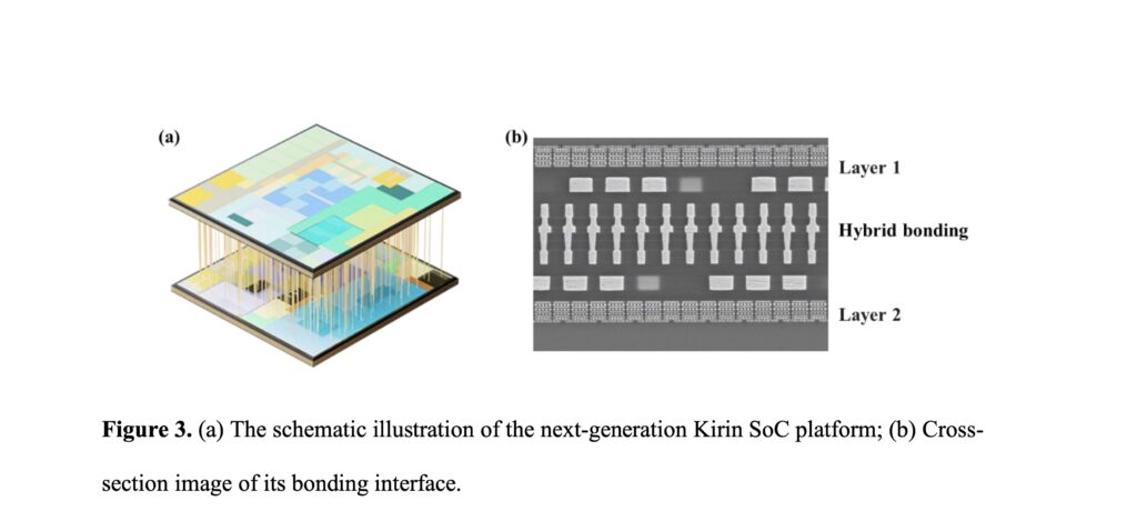
Huawei is presenting the Kirin 2026 not just as a new generation of mobile chip. At least on paper, it’s a demonstration that there’s still room to improve performance, density, and efficiency without solely relying on shrinking nanometers. The key lies in an idea that is beginning to gain importance across the industry: if scaling horizontally becomes more challenging, it’s time to scale vertically.
A technical document published by Tingbo He, Huawei’s head of the semiconductor business, describes a methodology called LogicFolding, based on dividing digital, analog, and memory circuits into stacked active layers connected via wafer-to-wafer hybrid bonding. This approach is part of a broader theory Huawei calls τ scaling, which measures progress not just by transistor size but by reducing the time data takes to move and process within the system.
The industry’s reading is clear. Huawei remains constrained by limited access to the most advanced lithography, but tries to compensate partly through advanced packaging, 3D integration, and dense vertical interconnections. It’s not a magic shortcut to TSMC’s 3 nm process, but a way to extract more performance from mature nodes.
What is LogicFolding and Why Does It Matter
For decades, chip advancement was explained by a simple idea: making transistors smaller. This approach enabled higher density, better performance, and lower cost per transistor. But Huawei’s own documentation states that this phase has partially exhausted itself, especially beyond 7 nm, where transistor costs no longer decline as quickly and design complexity skyrockets.
LogicFolding adopts a different approach. Instead of placing all chip blocks on a single flat surface, it distributes some logic and memory across multiple active layers. These layers are connected through hybrid bonding—a technique that directly joins metallic surfaces, usually copper, with a much smaller separation than traditional microbump methods.
The physical advantage is clear. If two blocks that were previously spaced millimeters apart now communicate through micrometers, the signal travels a shorter distance. This reduces delays, cuts power consumption, and enables higher bandwidth between chip sections such as CPU, GPU, NPU, caches, SRAM, and internal data routes.
Regarding the Kirin 2026, Huawei claims that hybrid bonding achieves a pitch of 1.5 micrometers, and that the design has been selectively applied to critical routes, not across the entire SoC. In other words, the first version will be conservative: it won’t fold the entire chip but will focus on areas where distance reduction adds the most value.
| Metrics Cited by Huawei | Kirin 9030 Pro | Kirin 2026 |
|---|---|---|
| Architecture | Planar | LogicFolding |
| Transistor Density | 155 MTr/mm² | 238 MTr/mm² |
| High-Performance Core Frequency | 2.75 GHz | 3.1 GHz |
| Normalized Power at Equal Performance | 1 | 0.59 |
| Voltage at ISO-Performance Test | 1.1 V | 0.9 V |
According to Huawei, transistor density increases by 55% in one generation, while power consumption for the same performance drops by 41%. In SRAM, Huawei claims a more than 40% improvement in operational frequency. In a typical core, the double-layer design reportedly reduced clock buffers by over 50%, clock skew by 25%, and wiring length by around 30%.
These figures are impressive, but should be interpreted with caution. They come from Huawei’s technical documentation, not independent product testing. Moreover, the document acknowledges that thermal management remains a major challenge for this architecture.
It’s Not Just Better Packaging, It’s Chip Redesign
An interesting aspect of LogicFolding is that it doesn’t simply stack memory or caches on top of logic, as some industry solutions do. Instead, its more ambitious goal is to treat multiple active layers as a single, continuous design space.
This requires changing tools, methodologies, and design rules. The document explains that if the vertical connection pitch is too wide, designers can only distribute large blocks across layers, as if assigning entire pieces to different floors. But if the pitch is sufficiently small, optimization can occur at a much finer level, approaching a near-continuous distribution of cells and routing between layers.
Huawei emphasizes that maintaining a low relationship between the hybrid bonding pitch and the top metal pitch is critical. For Kirin 2026, they mention a bonding pitch of 1.5 micrometers, with the goal of approaching a 1:1 ratio in the future. The denser this vertical connection, the less “overhead” there is when crossing from one layer to another.
However, implementing this isn’t just an idea; it demands sub-0.5 micrometer alignment precision, very compact Through-Silicon Vias (TSVs), intelligent redundancy to prevent small faults from degrading performance, and advanced EDA tools capable of closing timing in three dimensions. The document itself identifies 3D toolchains as one of the biggest open challenges for the next decade.
A Response to Sanctions, But Not a Complete Substitution for EUV
It’s tempting to see the Kirin 2026 as Huawei’s way of “bypassing” the US technological blockade. The reality is more nuanced. Advanced packaging can significantly improve performance on a mature node, but it doesn’t automatically turn a mature process into one equivalent to the most advanced EUV nodes from TSMC, Samsung, or Intel Foundry.
What it can do is help narrow the gap. If a company cannot fully access EUV or leading-node processes, it has two options: wait, or enhance performance through architecture, packaging, memory, software, and advanced manufacturing. Huawei seems to be betting on the latter.
The document frames this as a paradigm shift. Instead of measuring progress solely by nanometers, it proposes optimizing data movement times across each layer—transistor, circuit, chip, and system. This approach makes sense for mobile devices but also for AI, where much of the power consumption and cost come from moving data, not just computing it.
In fact, Huawei connects LogicFolding to other AI-focused data center technologies like Unified Bus and Hi-ONE, an near-packaged optical engine capable of 8 Tb/s per module. The core idea is that the future of hardware isn’t just about shrinking transistors; it’s about reducing latencies and distances throughout the entire stack.
The Big Unknown: Actual Production, Heat, and Sustained Performance
Kirin 2026 could be an important milestone, but many questions remain. Demonstrating an architecture on silicon is one thing; manufacturing millions of chips with good performance, manageable costs, and stable thermal behavior in a smartphone is another.
Stacking active layers complicates heat dissipation. In a mobile device, where space is tight and power must be carefully controlled, performance gains can be meaningless if the chip can’t maintain frequencies consistently. Huawei claims to avoid folding high-power circuits and uses thermal planning to prevent hot blocks from being too close, but only the final product will prove how effective these measures are.
Software also plays a crucial role. An NPU closer to memory, more efficient caches, or a packed NoC can significantly help, but the user will only see benefits if the operating system, local AI models, apps, and power management software are all optimized to leverage this architecture.
The key point is that Huawei is setting a direction that impacts more than just their smartphones. The entire industry is exploring advanced packaging, 3D stacking, logic-memory integration, and shorter interconnections. Apple, AMD, Intel, TSMC, Samsung, SK hynix, and other manufacturers are already working on variants of this general idea: the future isn’t only about making transistors smaller but reorganizing the system to move data less.
If the Kirin 2026 arrives on the market with these characteristics, it won’t just be “another Chinese chip.” It will be a demonstration of how far a strategy based on 3D design and hybrid bonding can go when access to the latest lithography is limited. It may not fully close the gap with sector leaders but shows that competition is no longer only about process nodes.
Frequently Asked Questions
What is LogicFolding?
A Huawei methodology that distributes digital, analog, and memory circuits across stacked active layers connected via hybrid bonding to reduce internal distances and improve density, performance, and efficiency.
What improvements does the Kirin 2026 promise?
According to Huawei’s technical documents, the Kirin 2026 increases transistor density from 155 to 238 MTr/mm² and reduces power consumption for the same performance by 41% compared to the Kirin 9030 Pro.
Does this mean Huawei can now compete with 3 nm chips?
Not necessarily. LogicFolding can narrow the gap using advanced packaging but doesn’t directly equate to having access to the most advanced EUV nodes. They are different technological paths.
What’s the main risk of 3D stacking in smartphones?
Thermal management. Stacking active layers can improve internal communication but makes heat dissipation more challenging if the design isn’t carefully planned.
via: ChinaXiv
