
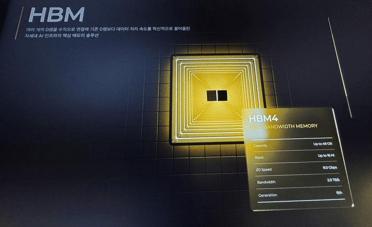
HBM memory has become one of the most contested components in artificial intelligence infrastructure. NVIDIA, AMD, major cloud providers, and accelerator manufacturers need increasingly faster, denser, and more efficient memory stacks to power high-performance GPUs and ASICs. But that race isn’t just about how many gigabytes fit next to the processor. It also depends on how the layers of DRAM are stacked, connected, and cooled.
Samsung Electronics and SK Hynix have been preparing the shift to hybrid bonding for some time, a packaging technology that promises reduced thickness, improved heat dissipation, and the enablement of denser internal connections. However, the industry is beginning to accept that its widespread adoption in HBM could be delayed beyond initial expectations. The reason is less spectacular than it seems: some of the advantages driving the urgency for change have lost short-term pressure.
What does hybrid bonding add compared to the current method
High Bandwidth Memory (HBM) is built by stacking multiple layers of DRAM and connecting them via vertical vias and advanced packaging technologies. Currently, the predominant method used is thermal compression bonding, which joins layers through heat, pressure, microbumps, and filler materials that provide mechanical support to the structure.
Hybrid bonding changes this approach. Instead of connecting layers with small metallic protrusions and filler materials, it directly bonds the copper interfaces of each layer. This allows for reducing the distance between components, increasing interconnection density, and improving electrical performance. It also helps to thin the final package by eliminating parts of the intermediate structure.
On paper, it aligns perfectly with the evolution of HBM. Each new generation demands higher bandwidth, more channels, more layers, and lower power consumption per transferred bit. HBM4, whose JEDEC standard was published as JESD270-4, doubled the interface width compared to HBM3E to 2,048 bits and was designed to support AI workloads and high-performance computing. (EDN)
The issue is that desirability doesn’t always mean it’s the best industrial choice at the right time. Hybrid bonding has advantages but also entails greater manufacturing complexity, new performance challenges, costs, and risks in a supply chain already operating at its limit due to demand for HBM.
Less urgency for thickness and temperature management
Initially, it was thought that Samsung and SK Hynix could introduce hybrid bonding with HBM4. Ultimately, the industry has continued to rely on more conventional joining technologies. Now, forecasts suggest that the transition might be delayed toward HBM4E, HBM5, or even later stages, depending on the number of layers and the actual needs of clients.
One reason is thickness. If the standard allows slightly thicker packages, the pressure to make each layer thinner decreases. In HBM3E, the height limit was more restrictive, but with HBM4, there’s room to accommodate configurations with 12 and 16 layers. Additionally, various industry reports indicate that future generations with more layers could relax the maximum allowed height again, providing more room for known technologies before forcing a switch to hybrid bonding.
The second factor is temperature. Hybrid bonding improves heat dissipation by eliminating lower thermal conductivity materials between layers, but Samsung and SK Hynix are exploring alternative approaches to address the same issue without drastically changing the entire bonding process.
At Computex 2026, Samsung showcased a proposal for HBM5 with Heat Path Block or HPB, a thermal structure designed to evacuate heat from critical areas of the package. SK Hynix, meanwhile, introduced iHBM, a solution based on Integrated Cooling Elements (ICE) integrated into the D2D PHY zone, which reportedly reduces thermal resistance by over 30%. (insights.trendforce.com)
This shift alters the equation. If manufacturers can enhance cooling with additional thermal structures and keep bonding processes mature, hybrid bonding becomes less of an immediate priority and more of a transition feature for when the design truly requires it.
Customer-driven timing
In HBM, decisions are not made solely by memory manufacturers. Key clients, especially those designing AI accelerators, influence the timeline. If NVIDIA, AMD, or major chip designers do not push for very high stacking configurations yet, memory providers have less incentive to assume the risks associated with early technology shifts.
Industry insights suggest that 12-layer products could continue to dominate even during part of the HBM4E cycle, while 16-layer and higher configurations might proceed more cautiously. This doesn’t mean the industry has lost interest in hybrid bonding; rather, the leap is being evaluated pragmatically: adopting it when benefits clearly outweigh the added complexity.
Underlying this is the reality that HBM today is among the most profitable and strategic memory market components. SK Hynix has established a very strong position in AI supply chains, Samsung is working to regain ground, and Micron is also a key competitor. In this context, a poorly executed process change can cost market share, performance, and customer confidence.
Advanced technology doesn’t always win if it arrives too early. In semiconductors, timing is often as critical as innovation. A solution must be mature, manufacturable, deliver sufficient performance, and meet actual customer requirements.
The main reason to adopt hybrid bonding will remain
Postponement doesn’t eliminate the trend. In the medium term, hybrid bonding still seems difficult to avoid. The key lies in I/O density. HBM4 already doubled the interface to 2,048 bits. If future generations further double internal connections, for example toward 4,096 I/O or stacks of 20 layers or more, physical space between terminals will shrink significantly.
Here, thermal compression bonding begins to show limitations. Microbumps take up space and can deform laterally during bonding. When connections need to be even closer, directly bonding copper surfaces may become the most logical route to maintain density, efficiency, and reliability.
That’s why Samsung and SK Hynix will continue investing in R&D for hybrid bonding. Although approaches like HPB, iHBM, and relaxed height specifications may provide margin for a generation or two, the technical direction of HBM points toward denser packages with greater thermal demands. At some point, interim solutions will no longer suffice.
The key takeaway is that the next AI battle will not only be fought on GPUs but also in memory packaging. HBM has become a bottleneck as significant as the chip manufacturing node or data center power capacity. If memory fails to deliver sufficient bandwidth with controlled power and thermal profiles, accelerators won’t reach their full potential.
Samsung and SK Hynix are not abandoning hybrid bonding; they are calibrating the right timing to introduce it without disrupting the current supply chain the market depends on. The question is no longer whether HBM will adopt more advanced bonding technologies, but at which generation the increase in I/O, layers, and heat will make the switch unavoidable.
Frequently Asked Questions
What is hybrid bonding in HBM memory?
It’s a packaging technology that directly joins copper connections between DRAM layers without relying on traditional microbumps. It enables higher density, thinner packages, and improved electrical and thermal properties.
Why might Samsung and SK Hynix delay their adoption?
Because the pressure to reduce thickness has eased, and both manufacturers are developing alternative thermal solutions, like HPB in Samsung and iHBM in SK Hynix, which could extend the viability of more mature bonding methods.
How does this relate to AI?
AI accelerators require enormous memory bandwidth. HBM is placed beside GPUs and ASICs to supply data at high speed. If the memory overheats or cannot scale in density, it limits overall system performance.
When will hybrid bonding become inevitable?
Probably when future HBM generations significantly increase internal connections and number of layers. If the industry moves toward 4,096 I/O or stacks of 20 layers or more, hybrid bonding will become more prominent.
via: zdnet
