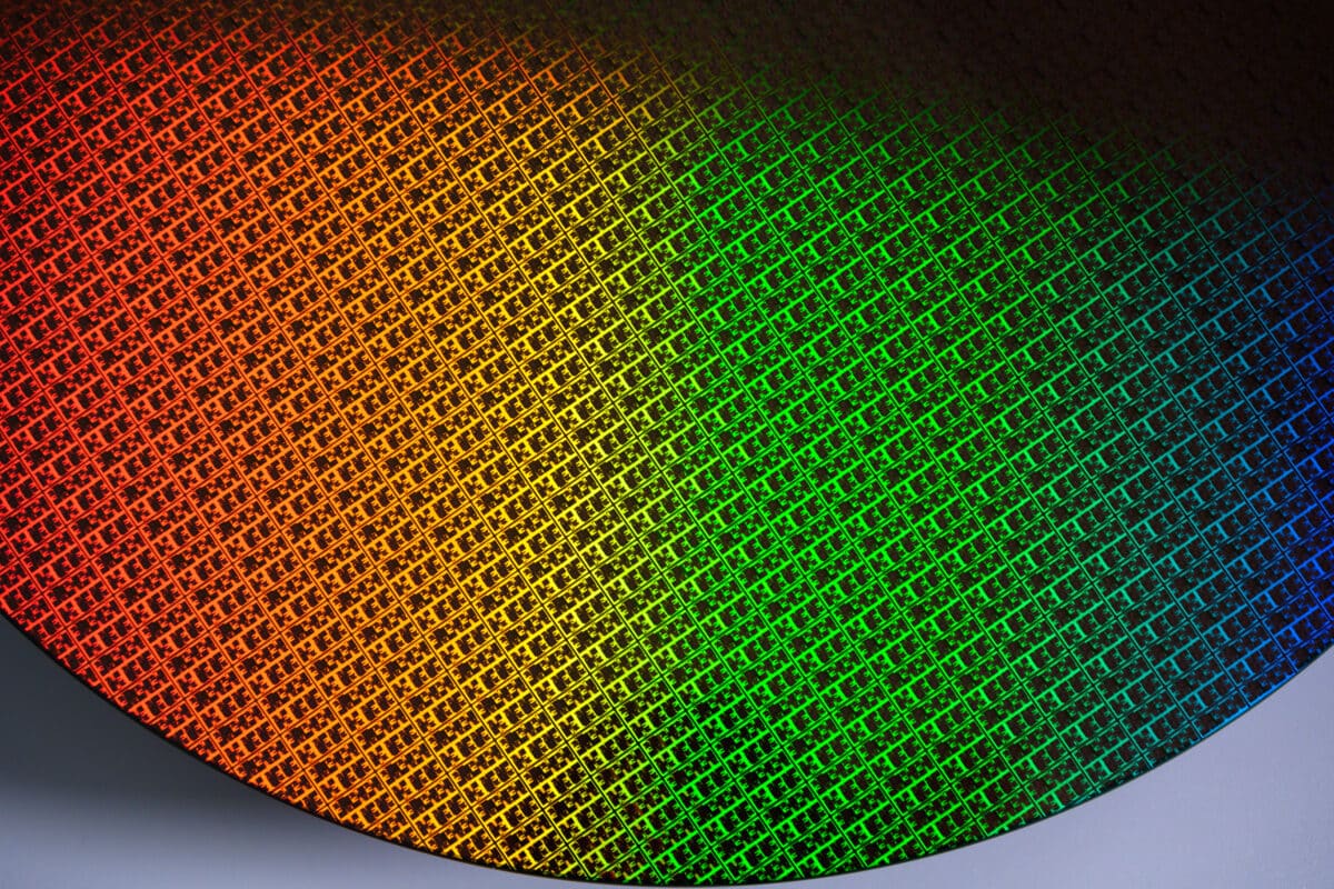
Intel seems to have overcome one of the most critical points of its industrial plan: the manufacturing performance of its 18A node. According to a report from Tom’s Hardware based on BlueFin Research Partners, the company has fixed the performance issues that had affected the process and is now reaching an approximate capacity of 30,000 wafers per month across its Oregon and Arizona facilities.
This news comes at a particularly sensitive time for Intel. The company needs to demonstrate that its advanced manufacturing business is back to being competitive and that the 18A node can support high-volume products, in addition to being attractive to external customers. It’s not just a technical matter: part of its industrial recovery, its foundry strategy, and the credibility of its upcoming processor generations depend on this process.
18A, the node Intel aims to regain trust with
Intel 18A is one of the company’s most important projects in years. The firm presents it as its significant leap in advanced manufacturing, with technologies like RibbonFET and PowerVia, its backside power delivery system. It is the node on which Intel has built much of its narrative of returning to the forefront of the semiconductor industry.
Intel has already indicated that Panther Lake, its upcoming platform for laptops, will be the first product based on Intel 18A, while Clearwater Forest will bring this process to the Xeon server market. Both products are manufactured at Fab 52 in Chandler, Arizona, a key facility for the company’s U.S. industrial strategy.
The reported capacity of 30,000 wafers per month, if confirmed in the terms published, is significant because it points to a more mature production phase. In semiconductors, having an advanced node on paper is not enough. The challenge is to produce enough functional chips with manageable costs and stable quality. Manufacturing yield — the output of usable chips per wafer — determines whether a technology can move from promise to business.
It’s worth noting, however, that Intel has not published an official yield percentage. The available information speaks of improved performance issues and an estimated production capacity but does not specify how many functional chips come from each wafer or the final cost.
Nova Lake, the big unknown for desktops
End-user interest hinges on what happens with Nova Lake, Intel’s upcoming desktop processor generation. Leaks suggest a much more ambitious design, with more cores and cache to directly compete with AMD’s Ryzen X3D series, which in recent years has gained advantages in gaming thanks to its 3D V-Cache.
This context is important. Intel is coming from a challenging period in desktops, marked by instability issues affecting some Core i9 models from the 13th and 14th generations and by competitive pressure from AMD in power consumption, efficiency, and gaming performance. Nova Lake is presented as a substantial response, but there are still more rumors than official data.
Some leaks speak of configurations with up to 52 cores and 288 MB of L3 cache, along with very high maximum turbo power consumption. These figures are eye-catching but should be treated with caution until Intel confirms the specifications, commercial models, actual performance, and release dates.
The 18A node could be a decisive factor, although it alone won’t solve all challenges. A competitive CPU also depends on architecture, cache design, frequencies, power consumption, platform, price, and availability. If Intel manages to combine a solid manufacturing process with a well-tuned architecture, Nova Lake could reintroduce pressure to the desktop market. If the product arrives late or with difficult-to-justify power usage, AMD will still have room to defend its position.
18A-P and 14A mark the next phase
As 18A progresses toward commercial products, Intel has already begun moving on to its next variant: 18A-P. The company announced in June that this improved process has entered risk production and promises up to 9% more performance at the same power or 18% less power at the same performance compared to 18A. It also maintains design rule compatibility, a key detail to facilitate adoption.
This step could be important for Intel Foundry. The company not only needs to manufacture its own processors but also convince external customers that its nodes are reliable, competitive, and predictable. In this business, technology matters greatly, but confidence weighs even more.
Behind it is 14A, Intel’s next major step, expected to utilize High-NA EUV lithography. The company has asserted that this node will be crucial for its future as an advanced manufacturer, but its success will depend on securing customers, investments, and sufficient volume. In chips, an ambitious roadmap only has value if factories turn it into real, profitable products.
The improvements in 18A do not resolve all debates, but they provide Intel with a critical signal. After years of delays, execution issues, and loss of leadership against TSMC and AMD on various fronts, any tangible manufacturing progress counts. The company now needs to prove it with processors on the market, sufficient availability, and results that convince both manufacturers and consumers.
Frequently Asked Questions
What does it mean that Intel produces 30,000 wafers a month at 18A?
It means that, according to published information, Intel has reached a significant manufacturing capacity for this node. However, it does not automatically indicate the actual performance per wafer or the final cost of the chips.
Will Nova Lake use Intel 18A?
Leaks suggest that Nova Lake will be linked to 18A or related variants, but Intel still needs to confirm final specifications, schedule, and commercial configurations.
Why is Intel 18A so important?
Because it is the node with which Intel aims to regain ground in advanced manufacturing, support products like Panther Lake and Clearwater Forest, and strengthen its Intel Foundry business against other manufacturers.