The race for artificial intelligence is reshaping the power map within the chip industry. For years, the conversation focused almost entirely on advanced nodes, wafer fab capacity, and the ability of companies like TSMC, Samsung, or Intel to produce increasingly dense silicon. While this bottleneck remains significant, it no longer alone explains who can deliver AI accelerators on time.
The new pressure point is lower down the supply chain: advanced packaging, HBM memory, ABF substrates, thermal testing, assembly, and final validation. In other words, everything that turns a set of chips, memory, and materials into a functional accelerator ready to be deployed in an AI server.
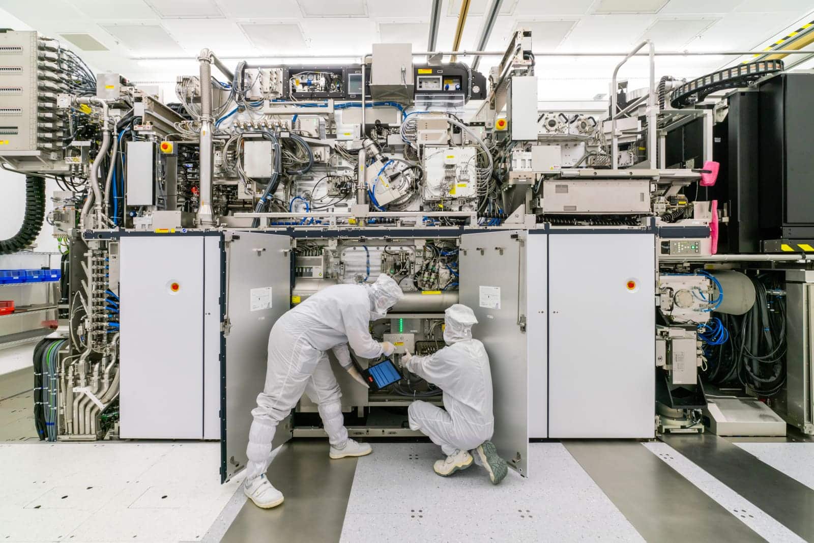
This is where OSATs come into play—short for outsourced semiconductor assembly and test—companies specializing in semiconductor assembly and testing. Their role has shifted from being a less visible part of the process to becoming a strategic element. According to DIGITIMES, cloud demand for AI is filling packaging orders through 2027, giving OSATs more capacity to negotiate prices in a market that was once more cyclical.
The bottleneck shifts from wafer to package
The reason is both technical and economic. Modern AI accelerators are no longer simple monolithic chips. They incorporate chiplets, multiple compute dies, HBM stacks, interposers, multi-layer substrates, and increasingly demanding thermal dissipation systems. While die manufacturing remains complex, the real challenge lies in integrating all these components with performance, bandwidth, energy efficiency, and reliability.
Santiago & Company summarizes it plainly: the AI compute advantage is no longer solely gained at the wafer fab but in the industrial infrastructure that transforms silicon into deployable systems. Their analysis states that the bottleneck has shifted toward the “physical integration stack”: advanced packaging, HBM, ABF substrates, testing capacity, and cooling.
The most striking data illustrating this shift is that the leading AI chip designers are projected to account for around 90% of the global CoWoS and HBM supply in 2025, despite using only about 12% of advanced logic die production. Put differently: silicon is not necessarily the main limiting factor. What’s scarce is the capacity to package it with high-bandwidth memory and turn it into a functioning system.
| Supply Chain Layer | Before | Now with AI |
|---|---|---|
| Fabrication Node | Main shortage focus | Still critical but no longer enough |
| HBM | Specialized component | Core requirement for AI accelerators |
| Advanced packaging | Integration process | Strategic bottleneck |
| ABF substrates | Opaque technical material | Cost and availability factor |
| Testing & burn-in | Final control phase | Actual product output gate |
| OSAT | External industrial service | Negotiation power capability |
This is why OSATs are gaining influence. If orders are committed far in advance and manufacturing capacity cannot be expanded overnight, those who have assembly, testing, and validation lines using advanced technologies can negotiate better. They no longer just sell “back-end services”—they sell access to scarce capacity.
CoWoS, HBM, and ABF: the acronyms explaining the bottleneck
The pressure is not confined to a single technology. TSMC has positioned CoWoS as one of the most relevant platforms for major AI accelerators. According to Santiago & Company, TSMC aims for an internal CoWoS capacity of 127,000 wafers per month by late 2026, while independent suppliers like ASE Technology could add approximately 40,000 wafers of additional capacity each month.
The issue is that much of that capacity is already committed. The same analysis indicates that NVIDIA is said to have reserved over half of TSMC’s projected CoWoS capacity for 2026-2027, with an estimate of 800,000 to 850,000 wafers to support its Blackwell Ultra and Rubin deployments. If this is accurate, developers of custom ASICs, smaller cloud providers, and other clients will be competing for remaining space.
HBM memory adds another layer of tension. AI accelerators need close integration of memory and compute to prevent bandwidth from becoming a limiting factor. This requires integrating multiple stacks of HBM diamonds with the logic die inside increasingly larger packages. IDTechEx notes that AI and HPC systems demand more compute dies, I/O dies, and HBM stacks within a single package—increasing the size of 2.5D and 3D platforms.
ABF substrates are another lesser-known bottleneck. A high-end accelerator canconsume up to ten times more ABF material than a standard PC processor, and multi-layer substrates can account for 30% to 40% of the package’s material costs in complex configurations, according to Santiago & Company. Furthermore, the supply chain is highly concentrated: Unimicron, Ibiden, and Shinko Electric are believed to account for around 75% of the global market for such substrates.
| Component | Why It Limits |
|---|---|
| CoWoS / 2.5D | Integrates logic and HBM on interposer or bridge |
| HBM | Provides bandwidth but supply is highly strained |
| ABF | Critical substrate for routing signals in large packages |
| Hybrid bonding | Enhances interconnect density but demands tighter process control |
| Panel-level packaging | Potential cost reduction but yield challenges remain |
| Thermal testing | Validates package operation under real load conditions |
The outcome is a chain where a failure in any component delays the entire system. GPUs aren’t useful if HBM is missing. HBM isn’t helpful if the packaging isn’t available. Packaging cannot be completed if substrates aren’t accessible. Assembly is pointless without testing and validation capacity.
More capacity but not in time for everyone
The industry is investing. TSMC, OSATs, memory suppliers, and substrate manufacturers are expanding capacity. But new lines don’t materialize overnight. In substrates, expansions can take 18 to 24 months due to equipment and cleanroom schedules. For advanced packaging, expansions also require machinery, mature processes, personnel, materials, and sufficient throughput.
IDTechEx predicts that advanced packaging for HPC will grow at a compounded annual rate of nearly 30% between 2026 and 2037. The consultancy also foresees larger packages, increased adoption of 2.5D and 3D stacking, greater interest in panel-level packaging, glass interposers, glass core substrates, hybrid bonding, and co-packaged optics. The direction is clear: packaging is no longer a secondary step but a platform for innovation.
This explains the pricing power of OSATs. If AI demand fills capacity through 2027, the market stops being merely tactical. Customers cannot wait until the last quarter to place orders; they must reserve capacity early, commit volumes, accept tighter terms, and in some cases, co-invest in capacity.
TrendForce anticipates that the severe shortage of 2.5D packaging could ease slightly in 2027, driven by backlog reductions and the expansion of TSMC’s CoWoS capacity. “Slight easing” doesn’t mean normalization; it suggests there might be some additional capacity buffer while demand for AI continues to grow and keep pressure on the supply chain.
Yield risk: when one failure fails the entire package
Advanced packaging introduces an additional challenge: the combination effect on yield. In monolithic chips, a defect affects only one die. In a heterogeneous package with logic, HBM, interposer, and substrate, a failure in any component can incapacitate the entire system. Early-stage yields are critical; low yields greatly increase the effective cost per functional unit.
Santiago & Company provides a clear example: in a $40,000 Blackwell system, a packaging line with a 60% yield would raise the effective cost per functional unit to approximately $66,600. This illustrates why testing, pre-screening for known-good dies, and thermal burn-in of several days are not secondary steps—they directly influence how many accelerators are actually ready for deployment.
For hardware buyers, this changes procurement strategies. It’s no longer enough to request chips; they must ensure assembly capacity, visibility into second- and third-tier suppliers, test reservations, risk sharing for scrap, and clauses that don’t leave all yield costs on the final integrator.
Impact on data centers and cloud services
The impact on the cloud market is direct. If packaging costs rise and capacity must be reserved years in advance, AI accelerators will take longer to arrive, cost more, and be less accessible. Hyperscalers with significant financial muscle can reserve capacity earlier. Smaller providers, in-house ASIC manufacturers, and companies building AI infrastructure outside the main supply chain will be at a disadvantage.
This will also influence service prices, GPU leasing options, cluster availability, and deployment timelines. The cost of AI isn’t solely determined by GPU prices—it depends on the entire physical chain that makes AI possible: packaging, memory, substrates, testing, cooling, power, and data center permits.
The chip industry is thus entering a less visible but more decisive phase. For years, we focused on nodes: 7 nm, 5 nm, 3 nm, 2 nm. Now, attention shifts to the package—how much HBM it contains, what interposer is used, which substrate is needed, what yield is achieved, where testing occurs, who has reserved capacity, and which OSAT can execute it.
AI is not only fueling GPU demand; it is reorganizing the semiconductor economy. In this new economy, back-end processes are no longer just final stages but become critical control points.
Frequently Asked Questions
What is an OSAT?
An OSAT is a company specializing in the assembly and testing of semiconductors. It operates after wafer fabrication, handling integration, packaging, and validation before the final deployment of chips.
Why does AI give pricing power to OSATs?
Because AI accelerators require advanced packaging, HBM, complex substrates, and rigorous testing. If capacity is fully booked until 2027, suppliers can negotiate better prices and terms.
What is CoWoS?
CoWoS (Chip-on-W wafer-Level-Stacking) is an advanced packaging technology from TSMC used to integrate logic chips and HBM memory into high-performance packages, widely used in AI accelerators.
Why are ABF substrates important?
They connect the advanced package to the system board and enable complex signal routing. In large AI accelerators, they consume much more material and can become bottlenecks.
Will the shortage be resolved by 2027?
It may gradually ease if new capacities come online, but it’s unlikely to fully disappear. AI demand, larger packages, and increased HBM usage will keep the pressure on the supply chain.