The race for mobile chips is no longer just about the manufacturing node. For years, the leap from one generation to the next was almost always explained by the same formula: more transistors, fewer nanometers, higher performance, and better power efficiency. That story remains important, but it’s starting to fall short. In high-end smartphones, the challenge is no longer just manufacturing a more powerful chip. It’s about keeping it fast inside an increasingly thinner phone, with less space and more heat buildup.
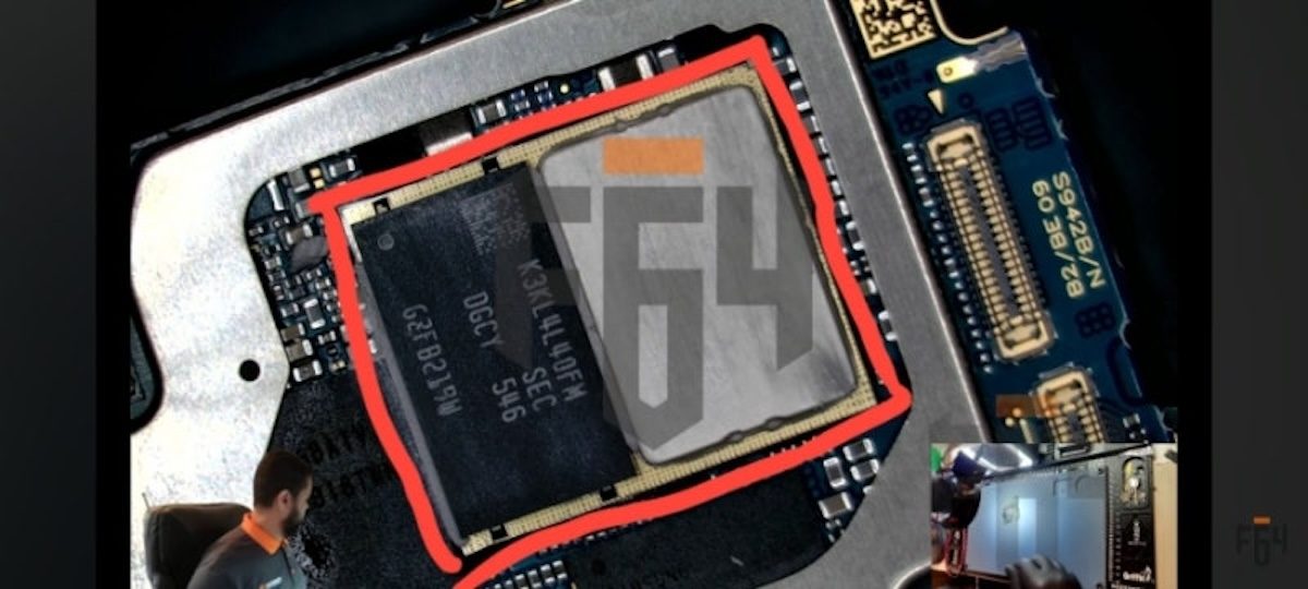
This is where Samsung aims to make a difference with the Exynos 2600. The processor has already attracted attention for its 2 nm process technology and for adopting Heat Path Block, a new packaging architecture designed to improve thermal dissipation of the SoC. Now, a leak from the Korean blog yeux1122 and reported by Wccftech adds another interesting detail: the LPDDR5X module associated with the Exynos 2600 would be roughly half the size of those used in other application processors, without apparent performance loss.
This data should be taken cautiously, as it doesn’t come from Samsung’s official technical sheet. But it aligns with a confirmed company trend: memory can no longer keep blocking the natural heat flow within the package.
The Limit of Package-on-Package
For years, mobile chips have used Package-on-Package structures, or PoP, where DRAM memory is placed on top of the application processor. The logic was straightforward: save space, reduce electrical distances, and fit CPU, GPU, NPU, ISP, modem, and memory into a volume compatible with a smartphone.
The problem is that this architecture has a thermal cost. The SoC generates heat at the bottom of the package, but the DRAM is on top. For heat to reach cooling elements like vapor chambers or internal heatsinks, it must pass through intermediate layers: solder balls, substrate, adhesives, encapsulation, and the memory structure itself. In a chip already handling AI workloads, gaming, computational photography, and advanced graphics, that path is becoming too narrow.
Samsung has explained this issue in its technical documentation on HPB. The company states that mobile packaging has evolved from being a simple protective layer for the chip to becoming a core technology for maintaining performance, controlling temperature, and freeing space inside the phone. The reasoning is simple: if power increases, temperature rises; if it rises too much, the chip reduces frequency to protect itself; and if it reduces frequency, sustained performance drops.
Heat Path Block aims to address this. Instead of letting the DRAM block the main heat dissipation route, Samsung repositions the memory module so it doesn’t overlap with the hottest zone. A copper-based metal block is placed on top of the processor, allowing heat transfer outward more quickly. According to Samsung, the Exynos 2600 reduces thermal resistance by up to 16% thanks to this solution and high-constant dielectric encapsulation materials.
| Element | Classic PoP Architecture | Exynos 2600 HPB Approach |
|---|---|---|
| DRAM Position | Above the processor | Repositioned to avoid hot zone blockage |
| Heat Path | Crosses memory layers and poor conductance materials | Exits through high-conductivity metal block |
| Goal | Save space and stay close to memory | Maintain performance and improve dissipation |
| Main Risk | Thermal limitation under prolonged load | Higher packaging complexity |
A Smaller LPDDR5X Changes More Than It Looks
The leak adds a detail that could be key to understanding Samsung’s strategy. According to the Korean blog, the LPDDR5X in the Exynos 2600 would have a speed of 10.6 Gbps, like other comparable modules, but a size roughly half. There’s also talk of a 15-pin configuration compared to 18 pins in another reference chip. In other words: less surface area occupied, without an apparent performance reduction.

If confirmed, this wouldn’t just be a design curiosity. Reducing the physical size of the DRAM helps reorganize the package around the processor. Less area dedicated to memory allows freeing space for the thermal block, improving the dissipation path, and keeping the entire assembly within the thickness constraints of a premium smartphone.
The key point is that Samsung isn’t just “making the RAM smaller.” It’s adapting memory, packaging, and dissipation as a system. That’s the interesting part. Modern mobile chips can no longer treat CPU, GPU, NPU, DRAM, and cooling as isolated pieces. Everything is connected through power, heat, space, and cost.
| Filtered data on Exynos 2600 LPDDR5X | Technical insight |
| Approximate size: half compared to other modules | More internal space to redesign the package |
| Speed: 10.6 Gbps | No bandwidth reduction due to size, according to the leak |
| 15 pins versus 18 pins | Potential connection design optimization |
| Exclusive to Exynos, per the source | Samsung may be leveraging vertical integration as an advantage |
It’s also mentioned that this custom DRAM type might be intended for Exynos and could continue in the Exynos 2700. That part remains highly speculative. Samsung has incentives to reserve some solutions for its own chips to strengthen Exynos’s competitiveness against Snapdragon and MediaTek. But it could also end up offering similar technologies to external clients if its advanced foundry and packaging business permits.
The Mobile Phone Enters the Era of Advanced Packaging
The broader trend goes beyond the Exynos 2600. The mobile industry is reaching a stage where packaging can weigh as much as the node itself. Moving from 3 nm to 2 nm helps, but doesn’t eliminate heat. On-device AI, ray-tracing gaming, advanced video recording, and sustained tasks put increasing long-term stress on the chip. Maximum peak performance for seconds isn’t enough anymore; what matters is how long the SoC can sustain high performance before throttling.
Apple is also heading in this direction, albeit with a different approach. Several leaks suggest their upcoming A20 chips might adopt a WMCM-type packaging, with memory placed next to the processor rather than on top. Qualcomm and MediaTek will also have to respond to this pressure, especially if upcoming Snapdragon and Dimensity processors increase AI performance and power consumption.
This shift resembles what’s happening in data center chips. In AI accelerators, GPUs, and HBM memory, advanced packaging has become a major industrial battleground. It’s not enough to design a good chip; you need to bring memory closer, improve interconnects, control heat, and manufacture the set to deliver sufficient performance. Smartphones, despite stricter space constraints, are now following similar logic.
Samsung’s advantage is that it controls multiple parts of this chain: designing Exynos, manufacturing memory, developing packaging, and operating as a foundry. That integration hasn’t always translated into mobile leadership. In fact, Exynos has suffered for years from a complicated perception compared to Snapdragon, especially regarding sustained performance, efficiency, and temperature. But if HPB and custom DRAM work as the design promises, Samsung could have a real opportunity to shift that narrative.
The question isn’t whether the Exynos 2600 will win all benchmarks. The more interesting question is whether Samsung has found a packaging architecture that provides more thermal margin for the phone without increasing size or sacrificing memory. If successful, the impact could go beyond a single Galaxy device.
The next-generation smartphone won’t just be a faster processor on a screen. It will be a piece of increasingly demanding thermal engineering. And in that race, moving memory a few millimeters might matter as much as shrinking the node by one nanometer.
Frequently Asked Questions
What is new about the LPDDR5X in the Exynos 2600?
According to a Korean leak, the LPDDR5X module in the Exynos 2600 would be roughly half the size of other comparable modules, maintaining the same speed of 10.6 Gbps.
Is this officially confirmed by Samsung?
Samsung has confirmed the Heat Path Block technology in the Exynos 2600 and its goal to improve thermal dissipation. The specific detail about the smaller LPDDR5X comes from leaks and should be regarded as unofficial information.
What is Heat Path Block?
It’s a packaging architecture that places a metal thermal block over the hot zone of the processor to transfer heat more efficiently to the phone’s cooling system.
Why does packaging matter in a mobile chip?
Because sustained performance depends on temperature. If heat isn’t effectively expelled from the package, the chip reduces frequency and performance in gaming, AI, camera processing, or prolonged tasks.
Could this technology reach Snapdragon or MediaTek?
It’s possible that similar solutions will spread across the industry, though Samsung’s specific custom DRAM or approach isn’t confirmed to be supplied to other manufacturers.