IBM has announced a 0.7-nanometer node chip technology, also described as 7 angstroms, and the reactions have quickly followed. The company promotes it as the industry’s first sub-nanometer development and as a way to continue increasing transistor density in the ongoing race for artificial intelligence computing. Elon Musk, however, has focused on the fine print: those 0.7 nm don’t mean the actual chip parts measure exactly 0.7 nanometers.
The critique hits a sensitive point in the industry. For decades, nanometers served as a simple way to explain advances in semiconductor manufacturing. The smaller the number, the smaller the transistor, the denser the chip, and theoretically, the better the performance or efficiency. But that straightforward relationship has not held for years. Today, a process node’s name functions more as a marketing and technological label than an exact physical measurement.
IBM does not hide this. In their own explanation, they acknowledge that, like with other recent advances, “7 angstroms” refers to a generation of chips built with a specific process, not to the width of the metal interconnects nor a single measurable dimension that could be accurately gauged with a nanometric ruler. Musk considers this naming convention potentially misleading and proposes naming nodes based on the number of atoms across the smallest feature’s width.
What IBM Has Actually Announced
IBM’s announcement isn’t just about trimming a number on the process label. The company describes a new architecture called nanostack, which stacks transistors in three dimensions instead of just shrinking them on a flat plane. The aim is to leverage vertical space to place more transistors in the same footprint, supporting density growth as traditional miniaturization approaches approach physical limits.
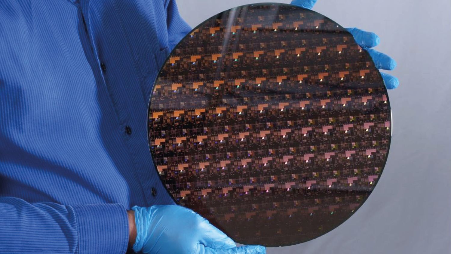
According to IBM, this technology allows nearly 100 billion transistors on a chip about the size of a fingernail—almost double the density of their previous 2 nm technology announced in 2021. The company also claims the new node can deliver up to 50% more performance or 70% better energy efficiency compared to their 2 nm chips. In SRAM memory, IBM reports a 40% scaling improvement, a significant figure because on-chip memory has become a bottleneck for AI workloads.
| IBM Announcement | Meaning |
|---|---|
| 0.7 nm / 7 angstroms node | New technological generation, not a single physical measurement |
| Nanostack architecture | Vertical stacking of transistors in tiers |
| Nearly 100 billion transistors | Higher density on a chip the size of a fingernail |
| Up to 50% performance increase | Compared to IBM’s 2 nm node |
| Up to 70% energy efficiency gain | Lower power consumption for equivalent capacity |
| 40% SRAM improvement | More dense embedded memory |
| Production possible in about five years | Not an immediate commercial technology |
While this advancement is significant, it should be viewed as cutting-edge research rather than a chip poised to arrive tomorrow in laptops or commercial accelerators. IBM has presented a technology and a manufacturing pathway, but has not yet announced a specific industry partner for large-scale production.
Why Musk Says the Name Could Be Misleading
Musk’s critique doesn’t necessarily deny the technical merit of nanostack. Instead, he questions its naming. Responding to a post on X, the entrepreneur argued that the industry should change its nomenclature and use a metric based on how many atoms wide the smallest feature is. In his view, this would be a more accurate way to describe the physical limits of the process.
The proposal is appealing because it grounds the language in tangible measurement. One nanometer equals ten angstroms, and the size of atoms is within the scale these technologies operate in. If a commercial label states “7 angstroms,” one might think there’s a main physical structure of that exact size. In reality, modern chips have many critical dimensions—gate length, channel, contacts, metallization, pitches, SRAM cell size, isolation layers, and packaging—all varying independently.
| Naming Approach | Advantages | Problems |
| Traditional nanometers | Simple, easy to understand | Does not represent an exact physical dimension anymore |
| Commercial node name | Useful for roadmaps and marketing | Can be misleading for the public |
| Transistor density | Close to practical results | Doesn’t directly reflect performance or efficiency |
| Atom count | Physically more intuitive | Difficult to standardize in complex architectures |
| Combined metrics | More comprehensive | Harder to communicate clearly |
Adopting Musk’s proposal isn’t simple either. A chip’s technology isn’t defined by a single “smallest feature.” Moreover, the current race isn’t solely about making transistors smaller. It involves stacking, reducing power, improving memory, changing materials, refining wafer bonding, optimizing interconnections, and producing with sufficient performance to make the process viable.
The Nanometer Era Ended Long Ago
The industry had already acknowledged this ambiguity. In 2021, Intel renamed parts of its process roadmap: what was previously 10 nm Enhanced SuperFin became Intel 7, and their 7 nm process was labeled Intel 4. The company explained this was to better align names with relative performance, efficiency, and density compared to competitors.
TSMC and Samsung also use node names that aren’t literal measurements. A chip built in 3 nm doesn’t have all features measuring 3 nm. The label indicates a generation with specific transistor types, design rules, density, power consumption, performance, materials, and lithography techniques.
Thus, Musk’s criticism has some validity, but recognizes that the entire industry already operates this way. The problem isn’t only IBM—it’s the entire language of advanced semiconductors. Names are retained because they serve marketing and roadmap purposes, even if they reveal less and less about physical reality.
The Real Advancement Is in 3D Stacking, Not Just Numbers
The most interesting part of IBM’s announcement is the move toward more complex 3D structures. Nanostack is seen as an evolution beyond nanosheets, which IBM had previously introduced as a basis for advanced nodes and which have started to penetrate the industry.
Stacking transistors allows increasing density without solely relying on size reduction in two dimensions. IBM describes techniques such as wafer bonding through ultra-thin dielectric layers, engineering of channels, and designing independently optimized NFET and PFET transistors. Translated: the chip resembles less a city spreading out across the land and more a city building upward in vertical layers.
This approach aligns with industry trends. Improvement doesn’t stem only from individual transistors but from the combined ecosystem of transistor, memory, interconnect, packaging, power, and software. In AI, where moving data consumes as much energy as computing it, reducing internal distances and improving memory can be just as crucial as adding more operations per second.
Implications for AI and Data Centers
IBM frames this announcement within the ongoing race for more powerful and efficient chips for AI, cloud infrastructure, and future devices. It makes sense. AI models require more computation, memory, and energy efficiency. An architecture that doubles density and cuts power use could greatly impact accelerators, specialized CPUs, embedded systems, and data centers.
However, many challenges remain between technological demonstration and stable industrial manufacturing. Issues include manufacturing yield, costs, wafer alignment, thermal dissipation, compatibility with existing tools, library design, validation, and partner adoption. Reuters reported that IBM expects possible production within about five years and that the company has licensed earlier technologies to Samsung and Rapidus, though no specific manufacturing partner has been announced.
| Outstanding Challenges | Why It Matters |
| Mass production | A single test chip isn’t enough for the mass market |
| Manufacturing yield | Too many defects escalate costs |
| Thermal management | Stacked transistors increase heat dissipation complexity |
| Design tools | Advanced libraries and tools are needed |
| Industrial partner | IBM researches but doesn’t produce consumer chips at scale |
| Cost | Adoption depends on economic viability of the leap |
The question isn’t just whether IBM can demonstrate the node. It’s who will produce it, for which customers, and at what cost per functional chip.
A Necessary Discussion for an Increasingly Opaque Industry
Musk’s open critique is timely. Chip manufacturing has become so complex that node names no longer offer a fair comparison among IBM, Intel, TSMC, Samsung, or Rapidus. A smaller number doesn’t always equate to a better chip for any workload. It might mean higher density but worse cost, or more performance but greater energy consumption. A better transistor may come with worse memory integration or a less feasible roadmap.
To the public, 0.7 nm sounds like science fiction. For engineers, the figure needs context. Manufacturers see it as a label designating a technology generation. Marketers use it to promote progress. Musk argues it’s a misleading convention that no longer accurately measures what it claims to.
IBM made a significant announcement but also subtly, perhaps unintentionally, highlighted the need for better communication about advances. In the angstrom era, lowering the number isn’t enough. It’s essential to specify what’s been reduced, how stacking has increased density, what real improvements in memory or energy savings have been achieved, and when such technology can be produced at a viable scale.
The nanometer was the magic word for chip progress for many years. Now, it’s starting to look like a label too small for a technology that’s already moving in three dimensions.
Frequently Asked Questions
Does IBM’s 0.7 nm chip actually measure 0.7 nanometers?
Not in the traditional sense. IBM acknowledges that “7 angstroms” indicates a manufacturing generation, not a single physical dimension as was the case many generations ago.
What is nanostack?
It’s a 3D transistor architecture that stacks and tiers structures to increase density and enhance performance or efficiency.
Why does Elon Musk critique the name?
Because he believes the node should be described by the number of atoms in the smallest feature, which he argues would be more precise.
When will we see commercial 0.7 nm chips?
IBM estimates about five years for potential production, but no industrial partner has yet been announced to manufacture this technology at scale.
via: wccftech