IBM has announced a major breakthrough in the semiconductor industry with the introduction of the first chips manufactured using sub-1 nanometer technology. The company has developed an innovative transistor architecture based on a 0.7 nanometer (7 angstroms) node, a milestone that marks a new step in the evolution of microprocessors at a time when traditional miniaturization approaches are nearing their physical limits.
Semiconductors are essential components for a wide range of technologies, from computers and mobile devices to transportation systems, critical infrastructure, and appliances. Therefore, any improvements in their capability and efficiency have a direct impact on multiple sectors.
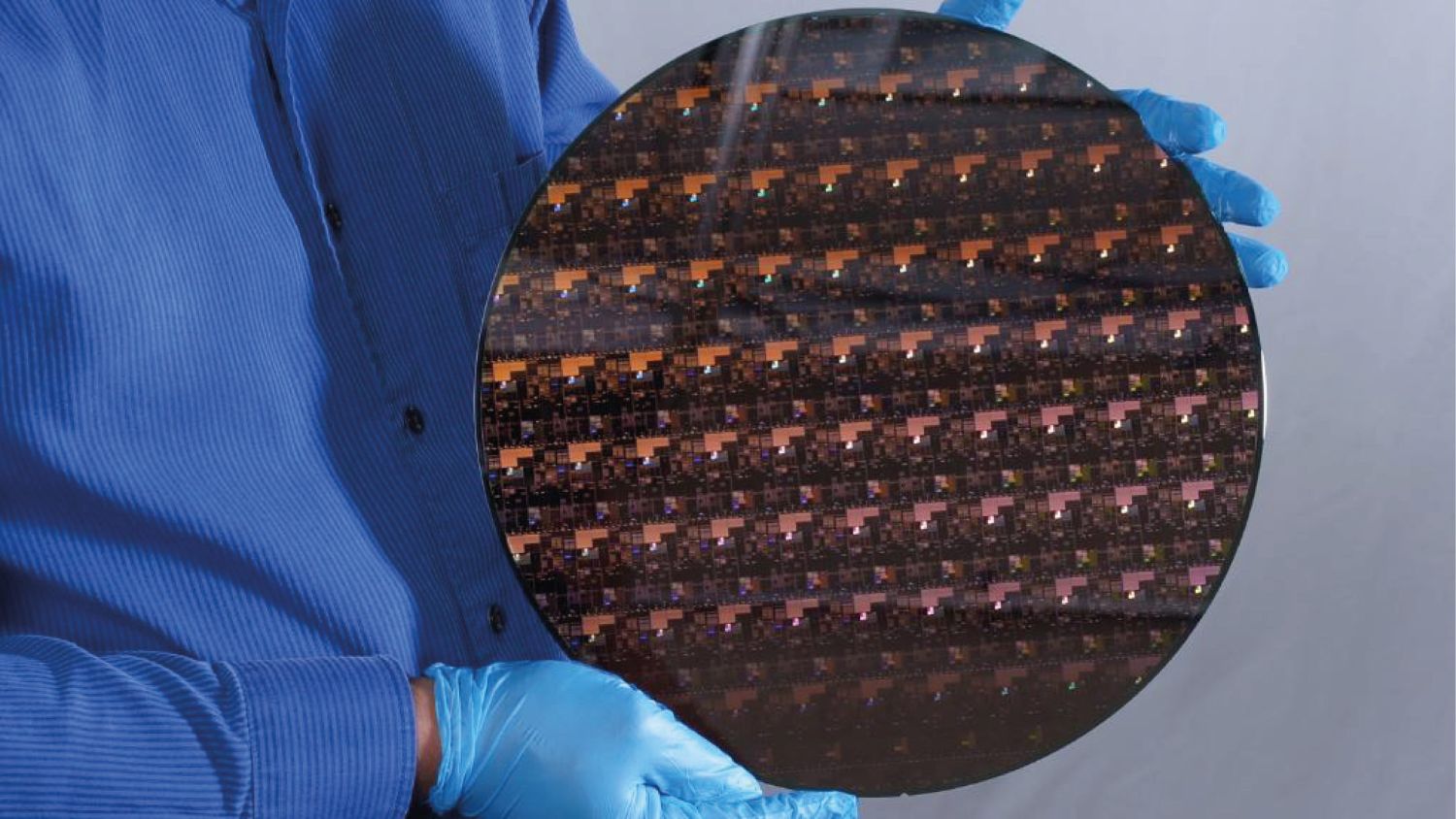
The new chip developed by IBM concentrates nearly 100 billion transistors in an area roughly the size of a thumbnail. This density is almost double that of the 2-nanometer chip the company unveiled in 2021. This advance was made possible through the incorporation of new materials and structural designs, including a three-dimensional architecture called nanostack, which allows continued performance increases even as components approach atomic dimensions.
According to technical data released by the company, this new generation of chips could offer up to 50% more performance or improve energy efficiency by 70% compared to previous 2-nanometer processors developed by IBM. These capabilities open doors to significant advances in areas like generative artificial intelligence, cloud computing, and the development of next-generation electronic devices.
With this announcement, IBM reinforces its commitment to semiconductor innovation and demonstrates that there are still new pathways to increase computing power and system efficiency for the future.
“IBM’s latest chip advancement marks a milestone in computing, taking technology beyond the nanometer era into the atomic scale. With our new nanostack architecture, we are not only manufacturing smaller transistors but also reimagining how chips are built to deliver substantially greater power and energy efficiency,” said Jay Gambetta, IBM Research Director and IBM Fellow. “This sector-leading innovation continues IBM’s legacy as a pioneer in next-generation technologies and lays the groundwork for the next era of computing.”
Nanostack: A Revolutionary Breakthrough in Chip Design
To manufacture this chip, IBM researchers developed a completely new transistor architecture called nanostack, the first three-dimensional nano-sheet-based design known in the industry. The nanostack represents a significant leap beyond current nano-sheet technology, which is IBM’s leading-edge architecture. The nanostack stacks and vertically arranges transistors, leveraging seamless 3D integration to concentrate more transistors on a single chip. It also enables the use of different material combinations within each stacked layer, optimizing the performance and energy efficiency of each transistor independently.
IBM’s nanostack architecture has been experimentally validated through ultra-thin dielectric junctions in CMOS integration, demonstrating double-channel engineering capability and functional operation of CMOS inverters with expected switching performance. These results confirm that nanostack technology can be physically constructed and is capable of performing real computations.
Additionally, in new research presented at VLSI 2026, IBM researchers demonstrated that nanostack architecture allows for a 40% reduction in SRAM, opening new possibilities for chip designers to create more efficient chips while meeting the high-bandwidth data demands of advanced AI workloads.
With this revolutionary structure, logic technology can extend below the 1 nm node for the first time, driving the era of angstrom-scale scaling where dimensions approach those of individual atoms. Although transistor nodes now refer to a manufacturing technology generation rather than an exact physical dimension, IBM’s 0.7 nm technology — also known as 7 angstroms — proves that continued scaling remains feasible. The nanostack architecture positions IBM’s semiconductor roadmap for at least a decade of future scaling.
Building on Decades of Semiconductor Innovation Leadership
This advance further demonstrates IBM’s leadership in semiconductor R&D. IBM has led the development of computer-driving chips worldwide for decades, from the first semiconductors in the 1960s to the world’s first 2 nm node chip. The company continues to pioneer in silicon technology, AI hardware, logic, and quantum processors to power the future of computing.
IBM and its partners are conducting this work at a leading semiconductor research center in Albany, New York, which will soon host a high numerical aperture extreme ultraviolet (High NAEUV) lithography team — vital for future logic circuit miniaturization. Developed by ASML, this technology enables ultraprecise circuit printing, facilitating the creation of smaller, more powerful chips. IBM, along with partners including Lam Research Corp. (Nasdaq: LRCX), Tokyo Electron (TEL), and SCREEN Semiconductor Solutions, Ltd., has been collaborating to develop new high-NA EUV processes and tools, which have already produced functional devices.
IBM has also recently announced a plan to create Anderon, the world’s first specialized quantum foundry. Anderon, an independent company spun off from IBM, will leverage IBM’s expertise in quantum computing and semiconductors to help position the United States as the leading manufacturer of quantum wafers worldwide.
With expectations that nanostack technology will be adopted as early as the sub-1 nm node, IBM predicts production could begin within five years.