Silicon is not about to disappear, but the semiconductor industry is already paving the way for a new era where simply reducing transistors using traditional materials will no longer suffice. The latest signals come from imec, ASML, and TSMC, demonstrating a route for integrating 300 mm wafers with transistors based on two-dimensional (2D) materials, featuring scaled nFET and pFET devices with contact pitch (CPP) down to 50 nm.
This advancement was presented at the IEEE/JSAP Symposium on VLSI Technology and Circuits 2026 and should not be interpreted as an imminent commercial chip announcement. Nonetheless, it is significant because it addresses one of the toughest challenges for the next decade: how to continue scaling logic when silicon channels approach increasingly physical limits. imec describes this achievement as an important step in the transition “from lab to factory” for transistors using 2D materials.
What imec, ASML, and TSMC have achieved
Their work focuses on TMD materials, or transition metal dichalcogenides, such as MoS₂, WS₂, and WSe₂. These compounds can form atomically thin conduction channels, allowing better control of the transistor as device dimensions shrink significantly. In theory, this makes them attractive candidates for extending the roadmap of advanced logic beyond current architectures.
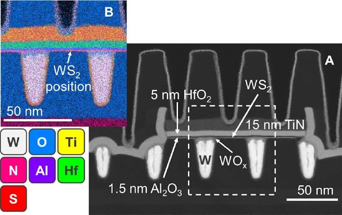
The demonstration combines nFET transistors with MoS₂ channels and pFETs based on WS₂ or WSe₂ on the same 300 mm platform. The key is not merely that they work in a laboratory setting—something the scientific community has shown for isolated devices for years—but that they are integrated with features closer to industry requirements and using tools compatible with advanced manufacturing.
Highlights include: nFET and pFET devices scaled to 50 nm CPP, very low off-current with gate voltages at 0 V in both polarities, and pFETs with WSe₂ channels showing performance near that of top laboratory devices. Additionally, imec reports 94% of transistors operational, defined as those with an Imax/Imin ratio exceeding 10⁵, indicating a stable process suitable for an experimental phase.
| Technical Element | Announced Result | Significance |
|---|---|---|
| Wafer type | 300 mm | Brings technology closer to industrial environments |
| Channel materials | MoS₂, WS₂, and WSe₂ | 2D alternatives to silicon channels |
| Transistor types | nFET and pFET | Essential step toward CMOS-like logic |
| Scaling | 50 nm contact pitch | Relevant metric for advanced nodes |
| Channel length cited | Up to 28 nm, per ASML | Shows role of EUV lithography | Operational performance | 94% of devices functional | Indicates robustness of the integration flow |
| Key tool | EUV single-pattern lithography | Enables finer, better-controlled structures |
| Future applications | Ultrascaled logic, BEOL, backside | Not limited to traditional front-end devices |
Why 2D materials matter for the angstrom era
The industry has exhausted silicon transistors for decades—initially with planar scaling, then FinFETs, and now gate-all-around architectures. The next step in density could involve CFETs, where complementary transistors are stacked vertically. Yet, these architectures encounter a common challenge: as the channel shrinks, maintaining good electrostatic control without degrading mobility, increasing leakage, or variability becomes more difficult.
2D materials offer a partial solution to this problem. Their extreme thinness allows the gate to better control the channel, even at very short lengths. This physical advantage can facilitate the fabrication of smaller, more efficient transistors. The industrial challenge has always been transferring delicate materials, forming low-resistance contacts, avoiding damage during processing, and doing all this on large wafers with tools compatible with real manufacturing environments.
This is the value of the recent announcement. imec, ASML, and TSMC have not only shown an exotic device; they have presented an integration pathway compatible with back-end processes for 300 mm wafers, with n- and p-type transistors on the same wafer and EUV lithography. ASML emphasizes that EUV resolution has enabled the creation of channels down to 28 nm and pitches suitable for advanced nodes, surpassing earlier demonstrations that produced larger or less representative features.
The architecture used is also significant. imec describes an “inverted” thin-film transistor fabrication flow, with bottom contacts and overlapping deposited gates. Instead of a conventional device structure, the TMD material is transferred onto pre-patterned tungsten trenches that serve as contacts. This approach helps preserve the integrity of the 2D channel and reduces contact-related issues.
It’s not the end of silicon, but a sign of change
‘Post-silicon era’ is an alluring phrase, but should be used cautiously. Commercial chips will still depend on silicon for a long time—both as the substrate and within the multiple layers of the process. Even if 2D channels reach advanced products, they will likely coexist with existing CMOS technology rather than replace it abruptly.
The industry itself works with long-term horizons. 2D materials are being explored as potential candidates for future nodes, for integration in backside applications, back-end-of-line architectures, and in designs where logic or memory are added closer to interconnects and power rails. Such integration could be particularly valuable in AI chips, high-performance processors, and 3D architectures, where moving data consumes increasing energy and space.
It’s also important to distinguish between demonstrating individual transistors and manufacturing complex commercial circuits. A functioning transistor is a single component. A chip requires millions or billions of devices with controlled variability, consistent performance, design rules, compact models, EDA tools, testing processes, and manufacturing chain compatibility. A recent review of 2D semiconductor technology highlights that bridging the gap from high-performance devices to functional integrated circuits remains a major challenge in the field.
The progress by imec, ASML, and TSMC builds on other recent industry work. For example, Intel and imec have already demonstrated 300 mm wafer-compatible modules for 2D transistors, with contacts and gate stacks geared for manufacturing. The common direction is clear: major companies are viewing 2D materials not just as academic curiosities but as viable pathways to sustain density and efficiency improvements as current architectures reach their limits.
TSMC and ASML’s involvement gives this work special significance. TSMC offers insights from the world’s leading foundry, emphasizing that any future technology must be integrable into repeatable, cost-effective processes. ASML contributes the role of EUV lithography as a precision tool to scale structures to meaningful dimensions. imec functions as a bridge to advanced research, where many promising ideas are trapped before reaching full-scale manufacturing.
For the market, this news does not alter the immediate roadmaps for CPUs, GPUs, or AI chips. Current and upcoming nodes will continue to rely on silicon-based transistors and gate-all-around architectures. However, it hints at what might come next: atomically thin channels, more aggressive 3D integration, and new materials designed to complement—rather than abruptly replace—the vast silicon infrastructure.
The semiconductor race is no longer just about making transistors smaller. It’s about finding materials that can still deliver performance as scaling becomes more challenging. In this regard, 2D transistors have taken an important step forward: from promising in the lab to demonstrating manufacturability, at least experimentally, through a process much closer to industrial reality.
Frequently Asked Questions
What is a 2D transistor?
It’s a transistor that uses an atomically thin material, such as TMDs like MoS₂, WS₂, and WSe₂, as the conduction channel. These are studied as potential alternatives to silicon for future nodes.
What have imec, ASML, and TSMC demonstrated?
They have showcased a 300 mm wafer integration route for 2D material-based nFETs and pFETs, with 50 nm contact pitch and promising electrical performance.
Does this mean silicon chips will stop being used soon?
Not in the near term. Silicon will remain central for years to come, serving as substrate and within multiple process layers. 2D materials are likely to augment future generations, especially as silicon channels hit physical limits.
When might 2D transistors appear in commercial products?
There’s no fixed timeline. Challenges remain in integration, variability control, contacts, circuit design, and large-scale manufacturing. This is an industrial research milestone, not an immediate product release.
via: imec-int