ASML is still deploying the first-generation High-NA EUV, but the semiconductor industry is already looking to the next step: Hyper-NA. This technology appears as a possible evolution of 13.5 nm EUV lithography, with a higher numerical aperture than current systems and a clear goal for chip manufacturers: continuing to print smaller structures without indefinitely increasing exposures, masks, and process steps.
The idea is simple to explain, though very difficult to produce. Current EUV scanners in the NXE family operate at 0.33 NA. The new High-NA EXE systems increase that to 0.55 NA and reduce resolution to about 8 nm, enabling the printing of features 1.7 times smaller and achieving transistor densities up to 2.9 times higher compared to NXE, according to ASML. Hyper-NA would take this further, with feasibility studies around 0.75-0.85 NA.
This isn’t a machine ready for installation tomorrow in a factory. Hyper-NA is still in the study phase and will depend on actual demand, cost, optics, depth of focus, masks, resists, metrology, and productivity. But its mere appearance on the roadmap signals something important: scaling doesn’t end at High-NA or the first 2 nm nodes. CPU, GPU, and AI accelerators manufacturing will continue to need higher resolution and less complexity per layer.
Why does numerical aperture change lithography?
In lithography, resolution largely depends on two variables: the wavelength of light and the optical system’s numerical aperture. EUV made a huge leap by using 13.5 nm light instead of the 193 nm used in the higher-resolution DUV lithography. Hyper-NA shifts the other major parameter: it increases the system’s ability to gather and focus light, allowing smaller pattern definition.
Hyper-NA would push that numerical aperture beyond 0.55 NA of High-NA. In theory, this improves resolution and image contrast—two critical factors for printing critical layers in advanced chips. The challenge is that each NA increase narrows the depth of focus, complicates optics, strains mask design, and forces a redesign of part of the manufacturing ecosystem.
| EUVM Generation | Numerical Aperture | Approximate Resolution | Expected Role |
|---|---|---|---|
| Low-NA EUV / NXE | 0.33 NA | 13 nm | Current production for advanced nodes |
| High-NA EUV / EXE | 0.55 NA | 8 nm | 2 nm, sub-2 nm, and advanced memory |
| Hyper-NA EUV | 0.75-0.85 NA in studies | Below High-NA | Future scaling and reduced multi-patterning |
| Beyond EUV | Wavelength less than 13.5 nm | Experimental | Longer-term alternatives |
This explains why ASML cannot stop at High-NA. Chipmakers need to print increasingly smaller lines, contacts, and structures. When a single exposure isn’t enough, they resort to multi-patterning: splitting one layer into multiple exposures or steps. It works, but raises wafer costs, lengthens production cycles, and increases defect risks.
The enemy is excessive multi-patterning
Advanced lithography is no longer just about making tiny patterns. It’s about doing so economically. When a critical layer requires several exposures, masks, and etching steps, each wafer becomes more expensive and slower to produce. Moreover, each additional step introduces new opportunities for errors.
High-NA aims to reduce this complexity by enabling the printing of structures in a single exposure that would require more intensive techniques at 0.33 NA. ASML argues that EXE can lower process complexity and increase wafer throughput by shortening cycles. Hyper-NA aims to extend that advantage once High-NA begins to reach its limits.
| Multi-patterning Problems | Impact on Manufacturing |
| More masks | Higher direct costs |
| More exposures | Longer time per wafer |
| More process steps | Longer production cycles |
| Greater alignment complexity | Overlay risks and cumulative errors |
| Potential defects | Lower yield |
| Higher energy consumption | Increased costs and environmental footprint |
For the end user, this doesn’t mean a Hyper-NA scanner will magically make CPUs or GPUs faster. Instead, it could allow manufacturers like Intel, TSMC, Samsung, and others to draw denser layers with fewer steps. If this translates into more transistors, better architectures, and controlled costs, then it could ultimately impact chip performance, power consumption, and price.
High-NA is still on its own ramp-up
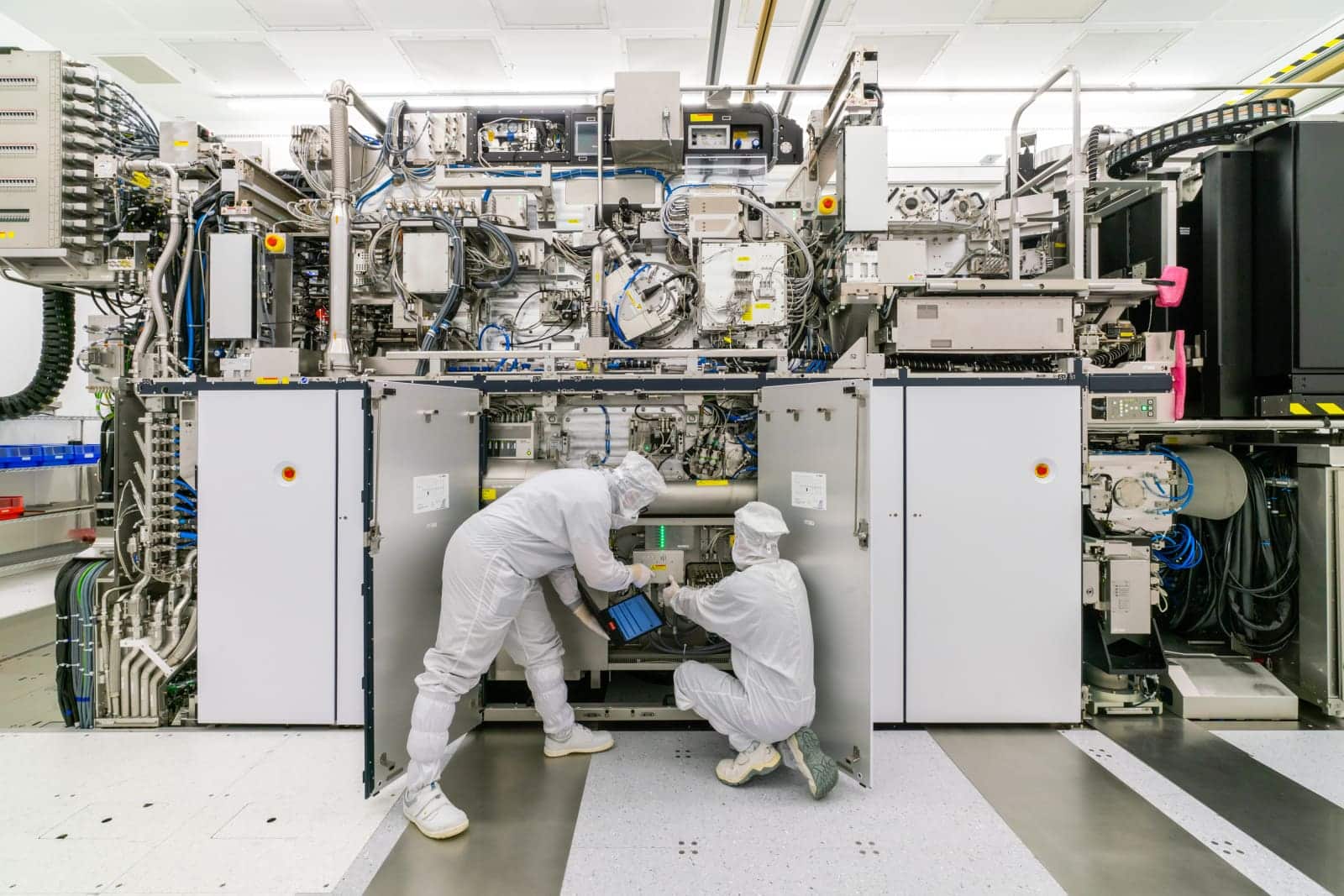
Before discussing Hyper-NA as a commercial product, it’s worth remembering that High-NA is still in early adoption. ASML delivered the initial modules of the TWINSCAN EXE:5000 to Intel in December 2023. The EXE platform uses anamorphic optics, increases NA from 0.33 to 0.55, and is designed for the most advanced logic nodes and similar-density memory.
Adoption is gradual because these machines are extremely costly, large, and complex. They also require adaptation of processes, masks, design, metrology, and manufacturing flows. Intel has been the most visible early customer, while TSMC, Samsung, and memory manufacturers are carefully evaluating the economic case for industrial deployment.
| Factors Influencing High-NA Adoption | Reasons |
| Scanner cost | Hundreds of millions of dollars per machine |
| Process changes | Requires manufacturing adaptations |
| Masks and design | Needs compatible workflows |
| Reduced exposure field | Requires faster steps to maintain productivity |
| Metrology | Must measure smaller structures |
| Node timing | Must align with each manufacturer’s roadmap |
| Cost per layer | Decides if the investment is justified over multi-patterning |
ASML claims that EXE can print over 185 wafers per hour and that its roadmap increases productivity even further. It also argues that High-NA reduces defects thanks to higher image contrast and allows for lower light doses per exposure, shortening layer print times. These are significant improvements, but industry decisions aren’t based solely on physics—they’re about total cost.
Hyper-NA: a response for the latter half of the next decade
Hyper-NA studies place the technology beyond High-NA, probably in the second half of the 2030s if the industry deems the leap worthwhile. The goal would be to extend EUV at 13.5 nm before considering even more radical alternatives, such as shorter-wavelength lithography.
The advantage of maintaining 13.5 nm is leveraging the existing EUV ecosystem: light sources, accumulated knowledge, materials, metrology, process design, and suppliers. Changing wavelength could offer a natural resolution improvement but would require rebuilding many components from scratch. Hyper-NA aims to stretch current EUV technology without jumping to an entirely different platform yet.
| Technology Roadmap | Advantages | Difficulties |
| Low-NA with multi-patterning | Matures ecosystem | More complexity and cost |
| High-NA | Better resolution with current EUV | High costs and industrial adaptation challenges |
| Hyper-NA | Higher resolution and less multi-patterning future | Depth of focus, optics, and mask challenges |
| Beyond EUV | Shorter wavelength | Lack of sources, mirrors, resists, and ecosystem |
| Advanced Packaging | Enhances performance beyond simple transistor scaling | Integration complexity |
The fundamental question is economic. Hyper-NA will be compelling if it can lower the total cost per layer compared to continuing with High-NA and multi-patterning. If machines are too expensive, too slow, or too hard to integrate, the industry might explore other options: smarter design, chiplets, advanced packaging, 3D-stacked memories, or complementary lithography.
CPUs, GPUs, and AI: why higher resolution is needed
Modern processors no longer scale solely by frequency. CPUs, GPUs, and AI accelerators require more transistors, larger caches, specialized units, higher internal bandwidth, and improved energy efficiency. Achieving this demands reducing dimensions in critical layers and combining miniaturization with new architectures.
AI adds pressure because training and inference chips are massive, costly, and highly sensitive to performance per watt. Each improvement in density helps incorporate more compute units, additional nearby memory, or more interconnect logic. But if fabricating those layers involves too many steps, costs escalate rapidly.
| Chip Type | Benefits of Advanced Lithography |
| CPU | More cache, better efficiency, more transistors per area |
| GPU | More compute units and improved performance per watt |
| AI Accelerators | Increased density for matrices, interconnect, and control |
| Advanced DRAM | Smaller cells and higher density |
| Mobile Chips | Lower power consumption and more integrated functions |
| Chiplets | Densely packed dies combined with advanced packaging |
Lithography alone doesn’t address all limits of silicon. Heat, energy, design complexity, packaging, and memory also matter as much as nodes. But without advances in critical layer printing, the industry loses a key tool for continuing to increase density.
Europe maintains a crucial role in technology leadership
ASML is a European company, but its influence is global. Its EUV scanners are essential for manufacturing the most advanced chips. No other supplier currently offers a comparable commercial solution for production EUV lithography. That makes the Dutch firm a strategic player across the entire semiconductor supply chain.
Hyper-NA strengthens that position in the long term. If the industry maintains the EUV trajectory for another decade, ASML will continue to hold a central role. But this advantage also brings pressure: each generation of scanners must arrive on time, with sufficient productivity and at a cost that manufacturers can justify.
| Actors | Interest in High-NA and Future Generations |
| ASML | Maintain leadership in advanced lithography |
| ZEISS SMT | High-precision optics |
| Intel | Regain process leadership |
| TSMC | Adopt when costs fit their roadmap |
| Samsung | Compete in advanced logic and memory |
| SK Hynix and Micron | Advance in DRAM and AI memory |
| Imec | Validate processes and assess future feasibility |
Controlling this technology also has geopolitical implications. The US, Europe, Japan, South Korea, Taiwan, and China all recognize that advanced lithography defines which chips can be made and where. Export restrictions on EUV highlight how these machines are already strategic infrastructure.
Outstanding challenges yet to be addressed
Hyper-NA shows promise but also raises many questions. Higher numerical aperture reduces depth of focus, making it harder to maintain image quality amid tiny variations in wafer, mask, or process. It may also require new approaches in resists, masks, inspection, correction algorithms, and defect control.
Additionally, productivity will be critical. If a machine produces finer patterns but takes too long, the cost per wafer may not be justified. The success of Hyper-NA depends on matching resolution improvements with throughput, stability, availability, and reasonable integration into fabs.
| Hyper-NA Challenges | Why It Matters |
| Depth of focus | Less margin for process variations |
| Optics | Increased precision and complexity |
| Masks | New design and inspection requirements |
| Resists | Materials need to be more sensitive and stable |
| Metrology | Measuring smaller structures |
| Productivity | Cost competitiveness per wafer |
| EDA Ecosystem | Designs must accommodate new rules |
| System cost | Must justify compared to multi-patterned High-NA |
Therefore, don’t jump to conclusions. Hyper-NA does not guarantee cheaper or faster chips on its own. It is a potential tool to sustain the scaling of advanced manufacturing. Its value will depend on when it arrives, how much it costs, and whether it sufficiently reduces complexity over alternatives.
The future of EUV is driven by economics, not just physics
The semiconductor industry has pushed physical limits for decades. But each new generation is adopted only if economically justified. High-NA has already undergone that scrutiny, and Hyper-NA will face it even more.
ASML aims to demonstrate that patterning smaller features with higher aperture is possible. The next challenge is proving that manufacturers can adopt that in production with good yields and without making wafers prohibitively expensive. Intel, TSMC, Samsung, and major memory manufacturers won’t adopt Hyper-NA for elegance—they’ll do so only if it allows better manufacturing than High-NA plus multi-patterning.
The overarching message is that EUV still has room to grow. Moving from NXE to EXE already marks one of the most significant evolutions in modern lithography. Hyper-NA aims at the next: maintaining EUV as a core technology for future nodes beyond 2 nm, which demand higher resolution and fewer steps.
The coming decade won’t just be decided in CPU and GPU designs. It will also depend on cleanroom processes, mirrors, light sources, resists, masks, and scanners—costing hundreds of millions. Hyper-NA remains, for now, a technical promise, but also a sign that ASML is preparing an answer to the question all manufacturers will face after High-NA: how to keep scaling without turning every critical layer into a nightmare of multi-patterning.
Frequently Asked Questions
What is Hyper-NA EUV?
Hyper-NA EUV is a potential evolution of EUV lithography that would raise the numerical aperture above High-NA, with studies around 0.75-0.85 NA, to print even smaller patterns.
How does it differ from High-NA?
High-NA uses 0.55 NA and delivers about 8 nm resolution on ASML’s EXE platform. Hyper-NA aims for higher resolution and less reliance on multi-patterning in future generations.
Will it be available soon?
Not yet. Hyper-NA is still in feasibility studies. Its industrial adoption would occur later, likely once High-NA starts to reach its limits at subsequent nodes.
Why is this important for CPUs, GPUs, and AI?
Because it could enable the fabrication of denser layers with fewer lithography steps, which is critical for processors, GPUs, and AI accelerators requiring more transistors and better efficiency.