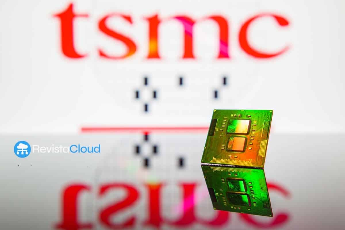
TSMC and Amkor Technology have signed a 10-year agreement to accelerate advanced semiconductor packaging in the United States. The partnership will allow TSMC to contract Amkor for advanced packaging and testing services in Arizona, a strategically important move to ensure chip manufacturing on American soil doesn’t rely on sending wafers to Asia for final stages.
The announcement comes at a time when the industry has recognized that making smaller transistors alone isn’t enough. AI chips, high-performance computing, automotive, and advanced electronics require integrating more memory, interconnections, and increased capacity within increasingly complex modules. This is where advanced packaging plays a key role—less visible than wafer fabrication but critical to the system’s final performance.
The collaboration combines two key investments in Arizona. TSMC is building its advanced fabs in Phoenix, while Amkor is expanding its packaging and testing campus in Peoria. The proximity of these facilities will enable a more integrated supply chain: silicon manufacturing, packaging, testing, and delivery within the United States.
Advanced packaging is no longer a secondary phase
For years, public discourse on semiconductors focused primarily on fabs, nodes, and lithography. But the AI boom has shifted the importance of each part of the chain. In many high-performance chips, packaging is no longer just the final industrial step; it is a technology that influences bandwidth, power consumption, latency, density, and cost.
TSMC and Amkor had already announced in 2024 a partnership to collaborate in Arizona, focusing on technologies like InFO and CoWoS—advanced packaging families used to integrate chips, memory, and high-performance components. The new 10-year deal provides greater business stability to this collaboration and reinforces the idea of a more complete local supply chain.
| Component of the alliance | Role within the chain |
|---|---|
| TSMC Arizona | Advanced wafer fabrication in Phoenix |
| Amkor Peoria | Advanced packaging and testing |
| End customers | AI, HPC, automotive, advanced electronics, consumer products |
| Packaging technologies | Advanced integration, system-in-package, wafer-level processing |
| Industrial goal | Reduce lead times and increase resilience |
| Agreement duration | 10 years |
The significance of this agreement can be better understood with a simple question: what’s the point of manufacturing advanced chips in the U.S. if they then need to be shipped overseas for packaging and testing? For years, Asia has concentrated much of the assembly, testing, and packaging capacity. The U.S. aims to correct this imbalance, and the TSMC-Amkor alliance directly targets that gap.
Arizona aims for a complete supply chain, not just fabs
Arizona has become a central hub in the U.S. semiconductor strategy. TSMC chose Phoenix to develop its advanced fabs, while Amkor has established its new advanced packaging and testing campus in Peoria. Both cities are close enough to facilitate a more efficient industrial flow.
In 2025, Amkor announced plans to expand its investment in Arizona to up to $7 billion in two phases. The project includes over 750,000 square feet of cleanroom space and could create up to 3,000 jobs once completed. The first phase is expected to be finished by mid-2027, with production beginning in early 2028, according to the company itself.
| Amkor Arizona project | Main data |
| Location | Peoria, Arizona |
| Total planned investment | Up to $7 billion |
| Phases | Two |
| Cleanroom size | Over 750,000 square feet |
| Potential jobs | Up to 3,000 |
| First facility completion | Mid-2027 |
| Expected start of production | Early 2028 |
| Clients cited by Amkor | Apple and NVIDIA |
This timeline indicates that the agreement will not have immediate effects across the entire chain. Plants need to be built, equipped, qualified, and scaled up. In semiconductors, this transition takes time. However, the strategic value lies in pre-establishing a commercial and technological relationship between the world’s largest contract manufacturer and one of the leading global providers of packaging and testing.
Kevin Zhang, senior vice president and deputy co-COO of TSMC, emphasized that both companies have extensive global collaboration experience. Kevin Engel, CEO of Amkor, described the deal as a step toward providing customers with a complete U.S.-based supply chain—from advanced silicon manufacturing to packaged and tested devices.
AI, CoWoS, and the growing pressure on packaging
The rising demand for AI accelerators has strained the global capacity for advanced packaging. Technologies like CoWoS are essential for integrating logic chips and high-bandwidth memory, a basic combination in GPUs and AI accelerators. The bottleneck is no longer just chip fabrication but assembling chips with the necessary memory and interconnections.
TSMC has invested heavily to expand its packaging capacity in Taiwan, but major clients also demand greater geographic flexibility. The U.S. wants a larger portion of this supply chain to stay domestic, especially for critical applications in AI, defense, cloud computing, automotive, and communications.
| Why advanced packaging matters | Practical implications |
| Integrates logic chips and high-bandwidth memory | Enhanced performance in AI and HPC |
| Reduces distances between components | Lower latency and power consumption |
| Enables more complex modules | Greater computational density |
| Affects time-to-market | Faster product cycles |
| Improves geographic resilience | Less dependence on Asia |
| Increases backend value | Test and packaging gain strategic importance |
This alliance also has a competitive angle. Companies like Intel, Samsung, TSMC, ASE, Amkor, JCET, and others are bolstering their packaging capabilities because the market is no longer decided solely by node technology. Advanced packaging has become a way to boost performance in an era where Moore’s Law is slowing and costs are rising.
A significant step in U.S. industrial policy
The TSMC-Amkor agreement aligns with Washington’s strategy to rebuild parts of the semiconductor supply chain domestically. The CHIPS Act has attracted investments in fabs, materials, equipment, and packaging, but turning announcements into sustained production remains the real challenge.
Chip manufacturing is a long chain. A wafer can leave a top-tier fab, but still requires sawing, assembly, interconnection, encapsulation, testing, and validation. Without proximity of these steps, the industrial cycle continues to depend on international routes, longer logistics, and exposure to geopolitical tensions.
| Previous situation | TSMC-Amkor in Arizona goal |
| Manufacturing in the U.S. and packaging in Asia | More critical steps within the U.S. |
| Higher logistical time | Shorter delivery cycles |
| Dependence on external capacity | Greater local resilience |
| Fragmented supply chain | Integration of fab and backend |
| Packaging as bottleneck | Dedicated capacity for advanced customers |
Talent will be a key challenge. Fabs are already competing for engineers, technicians, and process specialists. Advanced packaging also requires very specific profiles: materials engineering, quality control, automation, testing, cleanroom operations, reliability analysis, and production management. Arizona will need to train and attract enough personnel to sustain the announced growth.
A partnership that benefits clients too
For major chip designers, the agreement offers valuable continuity between fabrication and packaging. Companies like Apple, NVIDIA, AMD, Qualcomm, and other TSMC clients seek capacity, performance, and predictability. In high-volume or high-value products, reducing weeks of waiting can directly impact launches and availability.
Furthermore, Amkor is the largest OSAT based in the U.S. and one of the most prominent global players in packaging and testing. Its portfolio includes advanced packaging, wafer-level processing, and system-in-package solutions for mobile, data centers, AI, automotive, and wearables. TSMC provides the leadership in advanced fabrication; Amkor transforms these wafers into ready-for-market devices.
This does not mean the U.S. will quickly replace Asian capacity. Taiwan, South Korea, Malaysia, Singapore, China, and other hubs still possess significant scale, suppliers, talent, and experience. But it marks a concrete step where the American strategy was weakest: the advanced back-end.
The new chip map extends beyond the wafer
The TSMC-Amkor partnership highlights a often-overlooked reality: semiconductor sovereignty is not just about having fabs. A country may produce wafers, but if it doesn’t control materials, packaging, testing, equipment, software, talent, and customers, its autonomy remains partial.
The U.S. aims to close these gaps through public investment and industrial agreements. Arizona is becoming a testing ground for this approach, with TSMC focusing on manufacturing and Amkor on backend processes. If successful, this model could create a more comprehensive hub for advanced chips tied to AI and high-performance computing.
It also confirms that advanced packaging will be one of the major competitive fields in the coming decade. Manufacturers that can integrate silicon, memory, interconnection, testing, and local supply will have an advantage in markets where system-level performance matters more than just transistor count.
While the 10-year deal doesn’t solve all challenges in the U.S. chip supply chain, it provides a clearer route for manufacturing and packaging advanced chips within the same industrial corridor. In an industry shaped by AI and geopolitics, proximity like this can be as valuable as a new fab.
FAQs
What did TSMC and Amkor announce?
They signed a 10-year agreement to strengthen advanced packaging and testing of semiconductors in Arizona, within the U.S. chip supply chain.
Why is advanced packaging important?
Because it enables integration of chips, memory, and components into more powerful and efficient systems. It’s vital for AI, high-performance computing, automotive, and advanced electronics.
Where will the facilities be located?
TSMC is developing its advanced fabs in Phoenix, Arizona, while Amkor is building its packaging and testing campus in Peoria, also in Arizona.
When will Amkor’s campus start production?
Amkor indicated that the first phase should be completed by mid-2027, with production starting in early 2028.
Source: businesswire