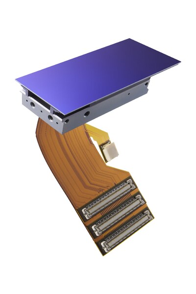
Sony Semiconductor Solutions has announced the upcoming launch of the IMX711, a direct-conversion X-ray CMOS image sensor with charge integration designed for inspection and measurement instrumentation. The company presents it as the fastest image sensor with the industry’s lowest noise, capable of reaching a maximum of 26,100 frames per second and precisely measuring X-ray energy over a broad dynamic range.
This innovation is not aimed at the traditional photography market, but at sectors where X-ray imaging is used to see what the naked eye cannot: semiconductor inspection, batteries, materials, crystal structures, industrial components, and scientific measurement. At a time when advanced manufacturing needs to detect smaller defects and analyze materials in greater detail, Sony aims to consolidate tasks that previously required multiple measurements or more complex setups into a single chip.
A direct-conversion sensor for measuring energy, not just images
The IMX711 directly detects X-rays and emits signals proportional to their energy. This technical distinction matters because it enables beyond conventional contrast-based imaging. The sensor can capture photon-level energy information and combine it with spatial data, opening possibilities to distinguish material differences, analyze constituent elements, and visualize two-dimensional distributions related to different energy levels.
Sony explains that the sensor uses a charge integration method that allows it to acquire photon energy information without pre-setting a threshold. In more conventional technologies, certain analyses might require multiple captures or more rigid pre-configuration. Here, the goal is to capture more comprehensive energy data for subsequent processing under various conditions.
Applications include high-speed inspection of moving objects, especially batteries and semiconductors; elemental mapping to differentiate photons of various energy levels; and simultaneous measurements of crystal structures and elemental analysis through photon energy and position data.
| Feature | Reported Data by Sony | Projected Impact |
|---|---|---|
| Model | IMX711 | X-ray CMOS sensor for inspection and measurement |
| Type | 3.73 | Large format for technical instrumentation |
| Area | 27.88 mm × 52.85 mm | Wide capture surface |
| Effective Pixels | Approximately 280,000 | Focused on measurement, not conventional photography |
| Maximum Speed | 26,100 fps | High-speed inspection and moving objects |
| Evaluated Noise | 34 e-rms | Better detection in low-flux conditions |
| Guaranteed Noise Value | 60 e-rms | Functional reference of the product |
| Mass Production | Q1 2026 | Scheduled industrial launch |
| Development | Sony Semiconductor Solutions and RIKEN | Transition from research to practical product |
More speed and less noise to detect weak signals
Speed is one of the main advantages of the IMX711. Sony states that it can reach 26,100 fps thanks to a proprietary circuit technology capable of suppressing charge saturation. By reducing the accumulated charge per frame, the sensor improves its behavior against saturation compared to conventional sensors.
This is especially important in industrial inspection because scenes don’t always have uniform brightness. Some areas may have strong signals while others are weak within the same measurement. A sensor with a larger dynamic range and lower noise can detect details that would otherwise remain hidden or be lost when adjusting exposure for the brighter zones.
Sony indicates that the random noise, a technical challenge for charge integration sensors, has been reduced to 34 e-rms under evaluation conditions. This allows for more reliable detection of faint X-ray signals and improves accuracy in low-flux scenarios. The guaranteed functional noise value is 60 e-rms, measured in an environment where the sensor’s internal operating temperature is at or below 20°C.
The combination of high speed and low noise can be especially beneficial in production lines where static high-quality images are not enough. For example, in batteries, inspection may need to observe internal layers, welds, or structures without stopping the process. In semiconductors, the challenge is to detect ever-smaller defects in components with complex geometries and high unit value.
RIKEN and Sony bring pixel structures into industrial applications
The IMX711 was developed through collaboration between Sony Semiconductor Solutions and RIKEN, one of Japan’s top research centers. According to Sony, the sensor builds upon a pixel structure invented by Dr. Takaki Hatsui of RIKEN. Using this foundation, both organizations worked on the technologies needed to turn the concept into a practical X-ray sensor.
The work included improving sensitivity, radiation resistance, and high-voltage tolerance. Sony contributed expertise in circuits, manufacturing processes, and packaging technology to move the design toward mass production.
This collaboration exemplifies a common pattern in specialized semiconductors: a concept originating in scientific research requiring years of engineering to become a reliable, manufacturable component for industrial equipment. For X-ray sensors, this transition depends not only on resolution and speed but also on stability, durability, calibration, noise, packaging, and irradiation performance.
The IMX711 also points toward an evolution in X-ray inspection toward richer data systems. The industry no longer only seeks to see if a part is broken or misassembled but aims to analyze composition, structure, phase changes, elemental distribution, and internal defects more quickly and with fewer steps. A sensor capable of capturing both energetic and spatial information on a single chip can simplify these workflows.
In scientific research, combining structural and elemental analysis can be useful for studying materials, crystalline structures, chemical processes, or samples where small variations matter. In industry, this can reduce inspection times and improve defect detection on high-value products.
X-rays for an industry that needs better measurement
The expected launch of the IMX711 occurs in a context of increased pressure on manufacturing quality. Advanced semiconductors, electric vehicle batteries, complex electronic devices, and new materials require faster, more precise, and more automatable inspection methods. X-ray imaging remains a valuable tool but must adapt to higher volumes and more demanding analysis requirements.
Sony is not introducing a sensor to replace all current X-ray systems but a component designed for advanced instrumentation. Its value will depend on how equipment manufacturers, laboratories, and industrial providers incorporate it. The fast speed of 26,100 fps, low noise, and photon-based energy measurement can be advantageous if they translate into faster equipment, more reliable measurements, or more comprehensive analysis.
Factors like cost, availability, and integration with existing systems will also be critical. In industrial and scientific markets, a new sensor is not adopted solely based on its specs; it requires compatible software, calibration, optics, readout electronics, support, and validation under real-world conditions.
Nonetheless, this announcement strengthens Sony Semiconductor Solutions’ position in specialized sensors beyond the consumer market. While known for its image sensors for cameras and smartphones, the IMX711 represents a different line: scientific and industrial sensors that leverage CMOS imaging experience for advanced measurement tools.
This development can be especially relevant where every hidden defect costs dearly. In batteries, internal faults can impact safety and longevity. In semiconductors, imperfections can invalidate high-value components. In research, more precise measurements can save time and improve data interpretation. The IMX711 aims to meet this need by capturing more information, faster, with less noise.
Frequently Asked Questions
What is the Sony IMX711?
It is a direct-conversion X-ray CMOS image sensor with charge integration, designed for advanced inspection and measurement instrumentation.
What speed does the IMX711 achieve?
Sony reports a maximum speed of 26,100 frames per second, claiming it to be the fastest among X-ray CMOS sensors with charge integration in the industry.
What applications is it intended for?
It targets semiconductor and battery inspection, elemental mapping, crystal structure analysis, scientific measurement, and energy-level difference detection at the photon level.
What advantages does it offer over conventional sensors?
It allows measurement of X-ray energy over a wide dynamic range and acquisition of photon-level energy information on a single sensor, with low noise and high-speed capture.
Source: prnewswire