Laser annealing is transitioning from a specialized technique within the semiconductor manufacturing to an increasingly important tool for three growth areas: silicon carbide power chips, over 400-layer 3D NAND memories, and advanced logic processes. The reason is simple: as materials become more difficult to process and structures grow deeper or smaller, applying heat precisely, locally, and for very short durations can mean the difference between a viable process and one that’s too aggressive for the wafer.
Annealing is a thermal treatment used to repair damage in the crystal lattice and activate dopants introduced through ion implantation. In conventional silicon, it has long been part of chip fabrication. The shift now is that the industry is applying it to materials and structures where traditional heating is more complex, such as silicon carbide (SiC), ultra-dense 3D NAND memories, or 2-nanometer nodes and beyond.
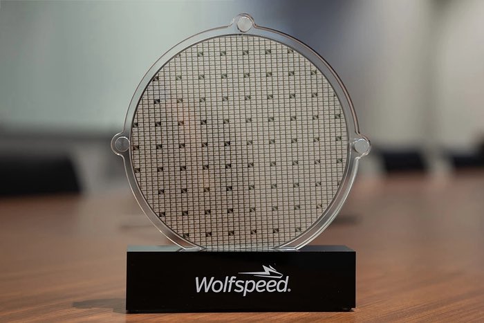
According to industry sources cited by South Korean media, Wolfspeed, one of the major players in the SiC wafer market, is moving toward adopting laser annealing equipment, with negotiations for an initial limited volume purchase that could expand later. This aligns with a broader trend: SiC is shifting to 200 mm wafers, and this transition requires more stable, repeatable processes that are compatible with high-volume production.
Silicon carbide forces a rethink of thermal treatments
Silicon carbide has become a strategic material for power semiconductors. It withstands higher temperatures, voltages, and demanding conditions better than traditional silicon, making it particularly attractive for electric vehicles, inverters, fast chargers, renewable energy, trains, industry, and data centers. Wolfspeed announced in 2025 the commercial launch of its 200 mm SiC materials portfolio, a significant step toward scaling this technology for larger-scale manufacturing.
The challenge lies in the process. While silicon may require anneals around 1,000°C, SiC can need temperatures exceeding 1,600°C to activate dopants and form proper electrical contacts. Such thermal levels pose risks: surface damage, interface defects, mechanical stresses, degradation of previously processed layers, and difficulties maintaining uniformity on large wafers.
Laser annealing offers an alternative because it allows heating very localized regions for extremely short times. Instead of exposing the entire wafer to prolonged thermal loads, the laser delivers energy precisely where needed. This reduces overall thermal budget and can help form ohmic contacts on SiC devices. Technical literature has already documented the use of laser annealing for back contacts in SiC power devices, precisely because of its ability to improve electrical contact without adding significant thermal load to the front side of the wafer.
The move to 8-inch wafers further emphasizes this opportunity. With SiC, increasing wafer diameter allows producing more chips per wafer and lowering unit costs, but it also amplifies issues like uniformity, defects, and process control. Larger wafers make precise and repeatable energy application even more critical.
Samsung is also reportedly reevaluating laser annealing within its strategy to enter SiC fabrication, with mass production expected around 2028 according to DigiTimes. If confirmed, this timeline indicates that adopting specialized SiC tools will be essential to competing with established players in high-power markets.
400-layer NAND: the new challenge is depth
The second front is 3D NAND memory. Manufacturers have been increasing the number of layers for years to boost capacity and reduce cost per bit. Moving beyond 400 layers presents increasingly difficult physical challenges: taller structures, deeper channels, more complex etching, and higher risks of electrical degradation or mechanical instability.
The key lies in the channel hole—the vertical channel connecting stacked cells. The more layers a NAND stack has, the deeper this channel must be. This complicates etching, uniformity, and electrical properties of the structure. If the channel isn’t of good quality, memory performance and reliability suffer.
Localized annealing can assist by selectively crystallizing specific regions of the channel. Instead of heating the entire structure, it targets areas where the material needs to improve electrical or structural properties. For NAND with over 400 layers, this capability can become a valuable tool for manufacturers aiming to scale further without making the process too fragile.
Samsung has reportedly completed development of 400-layer NAND technology and begun transitioning to production at Pyeongtaek, according to Business Korea. While each manufacturer follows its own path, the shared message is clear: NAND is entering a stage where increasing layers requires new process solutions, not just incremental improvements in etching and deposition.
This also has implications for artificial intelligence. The demand for storage in data centers, training, inference, multimodal models, and context memory is putting pressure on enterprise NAND. Large-capacity SSDs need higher density, efficiency, and reliability. If 400+ layer NAND becomes standard, technologies like laser annealing could gain prominence within manufacturing equipment landscapes.
2 nm nodes also boost the laser market
The third area involves advanced logic semiconductors. At 2 nm nodes and beyond, process margins are minimal. The industry must control dopants, defects, interfaces, and stresses with extreme precision. In such environments, conventional thermal treatments can be too broad or too aggressive for certain structures.
Some suppliers and manufacturers have already been using laser annealing in advanced processes. TheElec reported in 2023 that DIT supplies laser annealing equipment to SK Hynix, where this technology is used to repair wafer damage post-ion implantation. Although primarily related to memory, it illustrates how laser tools are increasingly present in advanced manufacturing lines.
The equipment market is also beginning to reflect this trend. Various industry analyses forecast growth for laser annealing equipment, especially for applications related to SiC. Although figures vary by firm, there is consensus that expansion will be driven by power chips, advanced memories, and more demanding logic nodes.
Challenges remain. Laser annealing requires fine control of energy, uniformity, speed, integration with process flow, and precise metrology. Poorly tuned processes can introduce new defects or variability. Additionally, each application has unique parameters: forming contacts in SiC differs from crystallizing a channel in NAND or activating dopants in advanced logic nodes.
For equipment manufacturers, expanding laser annealing offers an attractive market. For foundries and memory producers, it provides a way to address issues beyond what traditional lithography or etching can solve. For the semiconductor supply chain, this trend underscores a fundamental shift: each new chip generation demands more specialized processes that previously played a secondary role.
Laser annealing is not a new technology, but its time may be arriving now. SiC requires less aggressive thermal processes, 400-layer NAND demands more localized treatments, and 2 nm nodes tighten error margins. In all cases, heating less, better, and exactly where needed can become a key industrial advantage.
FAQ
What is laser annealing in semiconductors?
It’s a thermal process that uses a laser to heat specific regions of a wafer for very short durations. It repairs crystal damage, activates dopants, or modifies electrical properties without subjecting the entire wafer to high temperatures.
Why is it relevant for silicon carbide chips?
Because SiC requires much higher temperatures than silicon for certain processes. Laser annealing enables localized heating, reducing thermal stress on the wafer and existing layers.
How does it relate to over 400-layer NAND?
As 3D NAND stacks grow, the vertical channels become deeper and harder to stabilize. Localized annealing can help crystallize regions of the channel, improving electrical properties.
Can the laser equipment market grow?
Yes. The expansion of SiC, advanced NAND, and sub-2 nm logic nodes increases demand for more precise, scalable laser annealing solutions.
via: etnews