Intel is working to rebuild its credibility as an advanced semiconductor manufacturer by looking far beyond the next node. Lip-Bu Tan, the company’s CEO, has confirmed that Intel is already developing its future 10A and 7A technologies, two processes designed to succeed 18A and 14A over the next decade. The message is technical but also commercial: in the foundry business, having a competitive node today isn’t enough; customers want to know what’s coming next.
This announcement comes at a particularly delicate time for Intel. The company needs to prove that its third-party manufacturing division can compete with TSMC and Samsung, attract external customers, and execute a stable product roadmap after years of delays and losing technological leadership. In this context, 14A has become an important test. And 10A and 7A are a promise that Intel does not intend to stay stuck in a short-term recovery.
14A, the node that will determine if Intel re-enters the competition
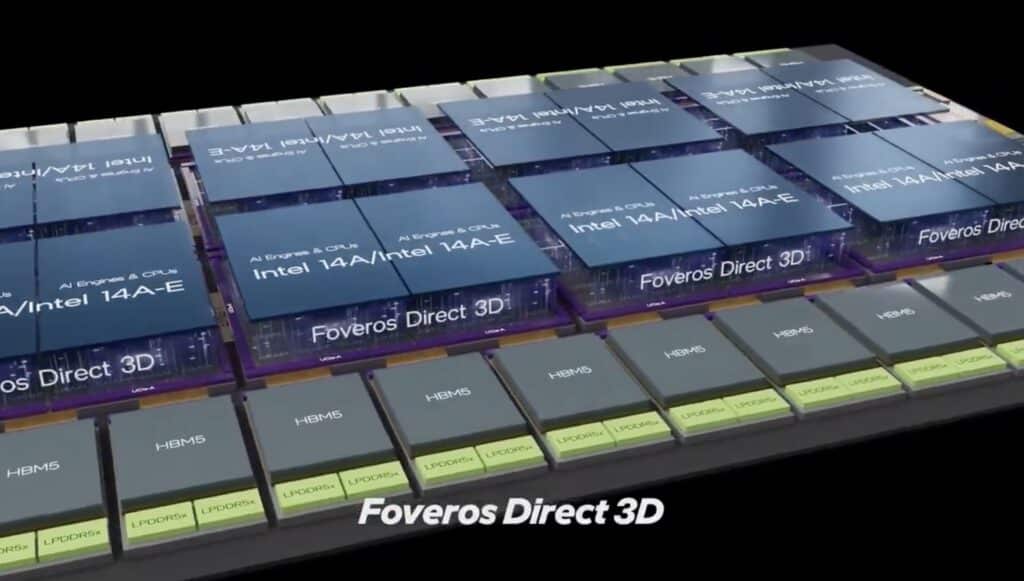
The immediate focus is on Intel 14A, a first-generation 1.4-nanometer manufacturing technology that will include RibbonFET 2 and PowerDirect, the second generation of backside power delivery. Intel also presents it as one of the first processes prepared to use ASML’s High-NA EUV lithography on selected layers, a key technology to continue shrinking dimensions without excessively increasing manufacturing steps.
Timing is critical. According to Lip-Bu Tan’s statements at the JP Morgan conference, Intel already has version 0.5 of the 14A PDK available, used by customers to start designing test chips. Version 0.9 of the PDK, considered much closer to a mature design environment, is expected in October for external customers, after an initial phase with internal teams.
A PDK, or Process Design Kit, is not a minor detail. It’s the set of rules, models, and libraries that enables a customer to design chips for a specific node. If the PDK arrives late, changes too much, or doesn’t provide enough confidence, the customer delays their product or moves to another supplier. That’s why Tan described it as a decisive piece: without a reliable PDK, there is no real foundry.
| Intel Node | Planned Role or Status |
|---|---|
| Intel 18A | Current advanced node and the foundation of its technological comeback |
| Intel 14A | Upcoming foundry node with RibbonFET 2, PowerDirect, and High-NA EUV support |
| PDK 14A v0.5 | Available for initial testing and prototype chips |
| PDK 14A v0.9 | Expected in October for external customers |
| 10A | Next-generation technology in early roadmap stages |
| 7A | The most advanced node in the publicly mentioned roadmap, according to Lip-Bu Tan |
The company states that several customers are engaged in discussions about 14A, although specific names have not been disclosed. This caution is understandable. For Intel, announcing interest without firm contracts can create difficult-to-sustain expectations. For customers, exposing intentions too early could compromise product strategies or negotiations with other manufacturers.
The race with TSMC won’t just be about timelines
Intel aims to begin risk production of 14A in 2028 and move to volume production in 2029, based on the information shared at the conference. This schedule places it near TSMC’s projected timeline for its A14 process. However, a direct comparison requires caution.
TSMC typically starts volume production with high performance and well-established manufacturing capacity. Intel, on the other hand, has traditionally used development fabs to start ramp-ups that take longer to reach maturity and comparable volume. This doesn’t mean Intel can’t compete; rather, the “production” dates don’t tell the whole story.
Furthermore, 14A and A14 are not identical on a point-by-point basis. Intel’s 14A is heavily oriented toward high-performance chips, data centers, and customers that benefit from backside power delivery and High-NA EUV lithography. TSMC argues that it doesn’t need High-NA EUV for A14 and can achieve performance, power efficiency, and density improvements with conventional EUV and refined architectures.
Intel’s approach is more aggressive from a technological perspective. High-NA EUV promises higher resolution and less multi-patterning in critical layers but also introduces risk. It’s not just about changing the lithography scanner; resins, photomasks, pellicles, metrology, design rules, computational lithography workflows, and complete process qualification also change. Achieving mass production with all these elements will be challenging.
10A and 7A: selling a decade, not just a node
Referring to 10A and 7A serves a strategic purpose. Large tech companies, chip manufacturers, and AI clients don’t choose a foundry just for a single product; they select a partner for multiple years. They need assurance that they can migrate from one node to another, that design rules will remain consistent, that advanced packaging options will be available, and that the provider has sufficient manufacturing capacity and a viable roadmap.
That’s what Lip-Bu Tan emphasized: customers aren’t just buying a process but a trajectory. Intel needs to demonstrate that 14A won’t be an anomaly but a platform upon which future nodes will be built. Although 10A and 7A are still in early development, they showcase ambition and continuity.
There’s also a geopolitical aspect. The U.S. seeks to regain advanced manufacturing capacity domestically and reduce dependence on Asia for critical semiconductors. Intel Foundry is a key part of this strategy, but to succeed, it needs external customers, scale, and execution capability. A long-term roadmap helps sell this story to governments, investors, and industry partners.
The challenge is that Intel no longer competes solely against other tech giants; it competes with the accumulated trust and reputation of TSMC. The Taiwanese foundry has built decades of reputation based on execution, performance, capacity, and close customer relationships. To shift a significant portion of that demand, Intel must do more than just demonstrate promising nodes: it must meet deadlines, stabilize yields, and prove it can manufacture complex chips for third parties reliably.
High-NA EUV: opportunity and risk
Adopting High-NA EUV could become a competitive advantage if Intel manages to deploy it successfully before other mass producers. Conversely, it could introduce added complexity if the technology takes longer than expected to mature.
ASML has already delivered next-generation High-NA EUV tools, and Intel was among the first to install these systems in preparation for future nodes. The promise is clear: pattern smaller features with greater precision and reduce the need for repetitive lithography steps. For AI chips, servers, and advanced accelerators, each improvement in density, power, and performance can have a significant economic impact.
But costs also increase. High-NA tools are expensive, the ecosystem is still evolving, and customers must trust that the process will be stable when their designs are ready. Intel has indicated that 14A will offer variants and options for different customers, which could be crucial if not everyone needs the most ambitious or costly process version.
This situation presents a paradox for Intel. To regain leadership, it must take technological risks. Yet, to attract foundry customers, it must offer stability, predictability, and competitive costs. 14A embodies this tension more than any previous node.
What’s at stake for Intel
The roadmap toward 10A and 7A shows Intel is planning for the long term, but the market will judge primarily on 14A. If the 0.9 version of the PDK arrives in October with sufficient maturity, and customers begin moving toward actual designs, Intel will have taken a significant step forward. If commitments are delayed or the node doesn’t impress, the recovery story could be questioned once again.
For the industry, Intel’s continued competition at the cutting edge is positive. More advanced capacity outside TSMC can reduce supply risks, improve options for AI customers, and strengthen supply chains in the U.S. and Europe. However, this diversification will only materialize if Intel Foundry demonstrates it can manufacture at the level it promises.
10A and 7A remain visions for the next decade. 14A is the closest test. In semiconductors, roadmaps matter a lot, but what truly influences the market are wafers leaving the fab with high yields, on time, and with customers eager to repeat orders.
Frequently Asked Questions
What are Intel 10A and 7A?
They are upcoming Intel manufacturing nodes that will succeed 18A and 14A within the next decade. They are still in early roadmap stages and are not yet production-ready technologies.
Why is Intel 14A so important?
Because it will be one of the key nodes where Intel wants to demonstrate that its foundry business can compete in advanced manufacturing for external customers.
What is a PDK and why does it matter?
A Process Design Kit (PDK) contains rules, models, and libraries needed to design chips for a specific process. Without a mature PDK, customers cannot confidently design for that node.
Does High-NA EUV guarantee that Intel will surpass TSMC?
No. High-NA EUV offers technical advantages but also adds costs and risks. Actual performance, yields, capacity, pricing, and customer confidence will ultimately determine success.
via: tomshardware