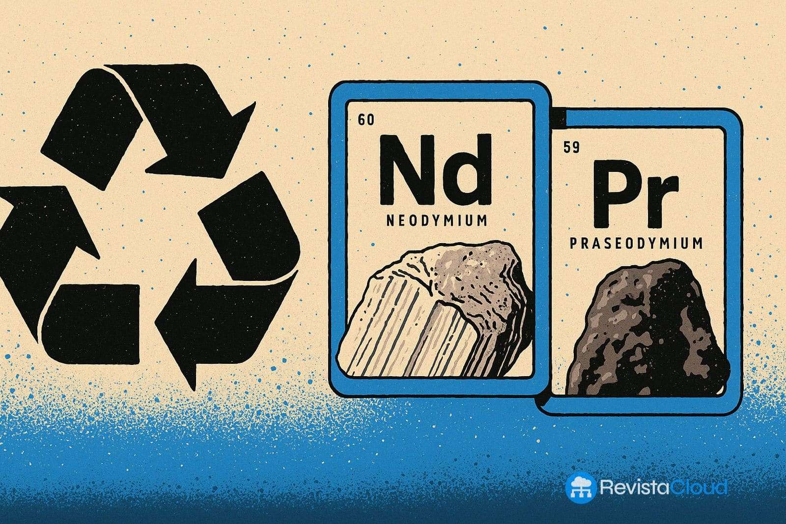
The rise of artificial intelligence is not only stressing the GPU market, HBM memory, or data centers. It’s also pushing materials much less known to their limits—materials that are essential for these infrastructures to communicate at the speeds demanded by the training and inference of large models. One of these is indium phosphide, known by its abbreviation in English as InP, a compound semiconductor used in lasers and high-speed optical devices.
China is beginning to move strategically in this market with intensity reminiscent of other strategic materials. It currently does not dominate the high-quality InP substrate segment, and technical barriers remain high. However, a combination of industrial investment, export controls, and soaring demand for optical modules in data centers has made this material a more sensitive component in the tech supply chain.
Why Indium Phosphide Matters for AI
Large AI clusters require moving tremendous amounts of data between GPUs, servers, racks, and data centers. This communication can no longer rely solely on copper. As interconnection speeds increase, optical modules of 800G, 1.6T, and future generations are becoming central to AI’s physical architecture.

This is where indium phosphide comes in. InP substrates are crystalline wafers used as the basis for laser chips employed in optical communications. Without these lasers, much of the high-speed connectivity needed by modern data centers would be far harder to scale. According to a forecast attributed by Global Semi Research to Goldman Sachs, shipments of 800G optical modules could exceed 34 million units in 2026, while 1.6T modules might surpass 25 million. While market estimates, these figures clearly indicate a trend: the internal network of data centers has become a core focus of AI infrastructure spending.
The relationship between optical modules and InP isn’t linear. EML (Electroabsorption Modulated Laser) solutions typically consume more substrate because they require multiple chips per module and relatively large die surfaces. Silicon photonics, on the other hand, can reduce the number of InP chips per module by using continuous-wave lasers as external light sources, but it doesn’t eliminate the dependency on the material.
From a technical perspective, the distinction matters. As CW lasers require more power for architectures like Co-Packaged Optics (CPO) and later Optical I/O (OIO), the chip size increases and wafer yields may decline. A 70- or 100-mW laser can produce many more units per wafer than a 300- or 400-mW source. If the market progresses toward more powerful lasers, silicon photonics might require fewer chips per module but at the expense of larger surface areas and more complex manufacturing controls. Material savings are not guaranteed.
Global Semi Research estimates that by 2026, demand could reach 100,000 to over 200,000 wafer equivalents of 3-inch wafers. This figure should be taken with caution since the market often mixes physical wafers, 2- and 3-inch equivalents, safety stock, and framework agreements that don’t always represent immediate actual consumption. Still, the market trend is clear: demand for InP related to AI is growing faster than the available quality wafers for advanced applications.
A Highly Concentrated and Difficult-to-Expand Market
The global supply of indium phosphide substrates is controlled by just a few players. According to Global Semi Research, Sumitomo Electric, AXT with its Chinese subsidiary Beijing Tongmei, and JX Nippon Mining & Metals control over 90% of the market. The same source estimates Sumitomo’s share at around 42%, AXT/Tongmei close to 36%, and JX about 13%. The issue isn’t just the total number of wafers but specifically the quality of 3- and 4-inch wafers suitable for demanding clients, especially semi-insulating substrates used in high-end optical applications.
Sumitomo Electric has acknowledged in investor materials that the increasing demand for optical devices for AI data centers is accelerating its capacity expansion plans. The company highlights that its main intra-data-center network products are EML and CW-LD lasers, and emphasizes its 4-inch mass production technology, along with high-power CW lasers of 350 mW or higher. It also indicates that it has expanded InP substrate capacity as part of its strategy for data center-related business.
AXT has also signaled that the demand cycle has shifted. In its first quarter 2026 results, the company reported revenues of $26.9 million, up from $19.4 million in the same period last year, linking InP demand growth to high-speed optical connectivity for AI data centers. Additionally, the company stated it completed a capital raise to support Tongmei’s capacity expansion and investment in products like 6-inch InP wafers.
AXT’s case is especially illustrative. Although it is an American company, it is based in Asia, with manufacturing facilities in China and stakes in Chinese raw material companies. This structure provides access to an integrated supply chain but also exposes it to export permissions and geopolitical tensions. In January 2026, the company lowered its revenue outlook for Q4 2025 due to issuing fewer export licenses for indium phosphide from China’s Ministry of Commerce than expected.
China announced export controls in February 2025 on products related to tungsten, tellurium, bismuth, molybdenum, and indium—materials with both civilian and military applications. The Chinese Ministry of Commerce presented these measures as part of its export control system, stating they are not outright bans but require licenses. For international clients, this difference can be significant: even if supply isn’t cut off, timelines, visibility, and inventory planning become more complex.
China’s Advantage Is Not Yet Secured
It’s tempting to see this move as a direct replication of other industries: China expands capacity, lowers costs, and displaces Western or Japanese competitors. While that could happen, indium phosphide is not an easy market. Producing high-quality wafers demands precise control over crystal growth, uniformity, defect levels, resistivity, and batch-to-batch consistency. Buying furnaces or building factories alone isn’t enough.
The main obstacle lies not just in investment but in accumulated expertise. For materials like InP, small process variations can ruin yields or prevent wafers from meeting the stringent requirements of advanced optical communications. Therefore, transitioning from initial production to reliable high-volume manufacturing for top-tier clients can take years, despite capital and industrial support.
It’s also important to distinguish between nominal capacity and usable capacity. A plant might declare a higher number of wafers per year, but the market needs specific substrate diameters and strict specifications. 2-inch wafers alone do not resolve the pressure for 3- and 4-inch wafers. While 6-inch wafers show promise for improving efficiency mid-term, they remain in R&D and pilot production stages in much of the industry.
Nonetheless, China’s opportunity is clear. If manufacturers can improve quality and volume, they could gain influence in a supply chain currently dominated by a few suppliers. For Beijing, InP aligns with a broader strategy: control over materials and components beneath the visible surface of AI chips, without which the infrastructure cannot scale properly.
For hyperscalers, optical module manufacturers, and network equipment providers, the message is less comfortable. GPU availability alone isn’t sufficient if optical connectivity becomes another bottleneck. Data center planning for AI must increasingly scrutinize the supply chains for lasers, substrates, and photonic components—beyond just electricity and servers’ capacity.
Indium phosphide has shifted from a niche, almost invisible material outside optoelectronics to a strategically critical component. AI is pushing data center networks toward speeds that demand more photonics, lasers, and high-quality wafers. China aims to capitalize on this demand to gain influence. Whether its manufacturers convert announced capacity into reliable, repeatable, and customer-acceptable production will ultimately determine success.
Frequently Asked Questions
What is indium phosphide, and what is it used for?
Indium phosphide is a compound semiconductor used in optoelectronic devices, especially lasers and high-speed optical communication components.
Why is it important for AI data centers?
Because AI clusters need to transfer enormous data volumes between GPUs and servers. 800G and 1.6T optical modules depend on lasers and components fabricated on substrates like InP.
Does China already dominate the InP substrate market?
No. The market remains concentrated among players like Sumitomo Electric, AXT/Tongmei, and JX Nippon Mining & Metals. China is expanding capacity but still needs to demonstrate quality and volume for advanced wafers.
Does silicon photonics eliminate dependence on InP?
Not entirely. Silicon photonics reduces some InP use in certain designs but still requires laser sources, typically based on III-V materials like indium phosphide.
via: Global Semi Research