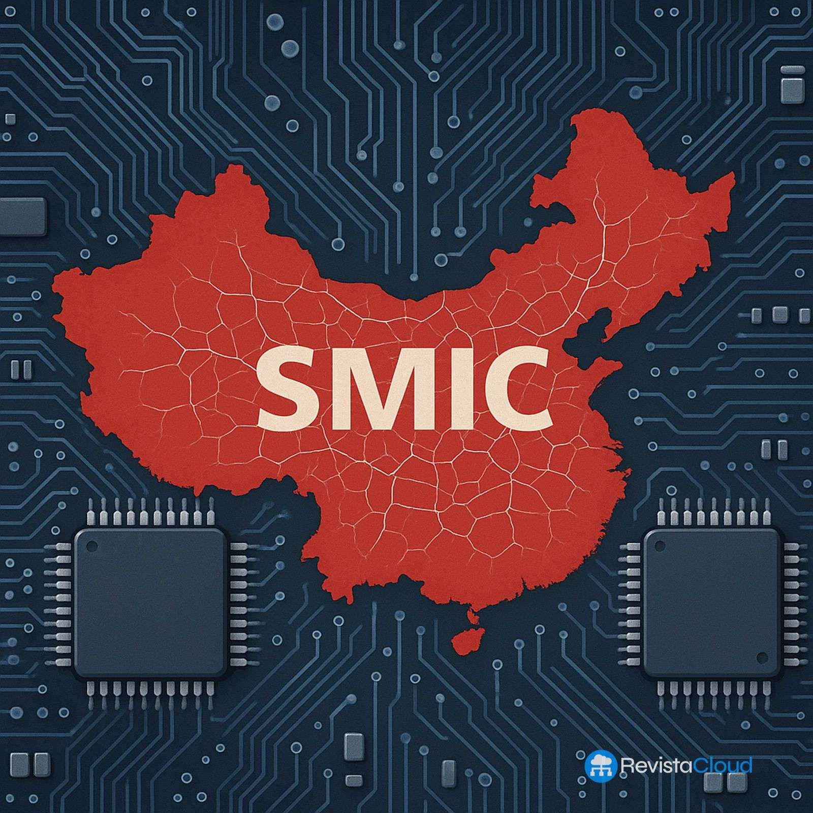
Zhang Rujing, founder of SMIC, has voiced a tension permeating the entire semiconductor industry: not all success is measured by reaching the 3 nm or 2 nm node first. In an interview covered by Chinese media, the executive argues that this perspective is a “conceptual error” because it reduces a vast market to a very visible, very expensive race reserved for just a few players.
This statement comes at a particularly sensitive time for China. SMIC is the country’s largest foundry, yet it remains constrained by restrictions on the export of advanced lithography equipment and the challenge of competing head-to-head with TSMC, Samsung Foundry, or Intel Foundry at the most advanced nodes. Therefore, Zhang’s thesis carries a dual meaning: it’s a reasonable critique of the obsession with cutting-edge technology, but also a pragmatic adaptation to the real limitations of the Chinese ecosystem.
Most of the market doesn’t operate at the advanced nodes
Zhang argues that, when analyzing the market by the number of products, advanced processes account for less than 20% of demand, while more than 80% comes from mature processes and specialized technologies. This serves as a reminder of something often lost in public discourse: many essential chips do not require 3 nm, 2 nm, or the latest lithography generations.
Automotive, industrial control, power electronics, sensors, microcontrollers, PMICs, connectivity, household appliances, wearables, machinery, IoT, and medical devices largely depend on mature nodes. These chips may not always make headlines but sustain entire supply chains. A car might need advanced chips for driver-assistance systems, but also dozens or hundreds of components made with much older processes. The same applies to factories, power grids, healthcare equipment, or production lines.
From this perspective, Zhang’s proposal makes industrial sense. China doesn’t need to win every race simultaneously to reduce reliance on external sources. It can achieve faster progress by identifying specific bottlenecks and developing capabilities in segments where it still depends on foreign suppliers: analog, power management, sensors, industrial communications, embedded components, and niche solutions.
This argument isn’t new, but it gains weight in the current context. The chip shortage during the pandemic revealed that mature nodes can halt entire sectors. It wasn’t just high-end GPUs that disrupted car manufacturing—controllers, power management chips, and seemingly less glamorous components were missing.
The issue is that “mature” doesn’t mean “easy.” Many special processes require know-how, quality control, materials, packaging, certifications, long-term reliability, and close relationships with industrial clients. In automotive or energy sectors, a chip isn’t replaced every six months. It must operate for years, withstand temperatures, vibrations, and demanding conditions. Entry barriers exist here as well.
AI: not everything depends on the big data center
Zhang’s second point pertains to artificial intelligence. The SMIC founder criticizes that a significant portion of China’s industry is overly focused on high-power chips for data centers—precisely the most challenging terrain: GPUs, training accelerators, large interconnections, HBM memory, advanced packaging, and clients with enormous budgets. Companies like NVIDIA, AMD, Google, Huawei, and major cloud platforms dominate this market.
For Zhang, Chinese startups should avoid entering this race without sufficient resources, given its requirement for massive capital, long cycles, and a highly complex supply chain. His alternative is distributed AI and edge AI: chips tailored for specific scenarios, close to users or machines, instead of always relying on the cloud.
This approach aligns with many real-world needs. AI will not only run on large clusters; it will also be embedded in industrial cameras, robots, vehicles, wearables, sensors, factories, medical devices, agricultural machinery, consumer electronics, and inspection equipment. In many of these cases, energy efficiency, cost, latency, security, and integration with specific hardware matter more than raw processing power.
That’s where China may have more room to maneuver. Competing against NVIDIA in training GPUs is one challenge; designing inference chips for industrial lines, EVs, or embedded vision devices is another. The latter markets may be less glamorous but could be huge if millions of units are involved.
They also provide a strategic advantage: it’s harder to block them with a single restriction. High-end AI accelerators depend on advanced nodes, HBM, 2.5D packaging, complex software, and highly concentrated suppliers. Edge AI, however, involves a broader array of processes, architectures, and use cases. This doesn’t eliminate dependencies but reduces pressure on the most sanctioned part of the chain.
The uncomfortable truth: TSMC is highly successful with advanced nodes
Zhang’s thesis should not be mistaken for a denial of the value of advanced nodes. TSMC proves just the opposite. In Q4 2025, its 3 nm node contributed 28% of wafer revenue, while 5 nm and 7 nm processes accounted for 35% and 14%, respectively. Overall, in 2025, technologies of 7 nm or below made up 74% of wafer revenue.
This explains why 3 nm and 2 nm matter so much. They are not the majority of products in volume, but they capture a large share of the economic value, margins, strategic customer attention, and control of critical segments like AI, premium smartphones, HPC, advanced networking, and high-performance CPUs.
TSMC also reports that its N2 technology, based on nanosheet transistors, ramped to volume production in 2025 as planned. This capability allows it to serve customers willing to pay for the latest: Apple, NVIDIA, AMD, Qualcomm, Broadcom, and other cutting-edge chip designers. The advantage isn’t just miniaturization but also delivering performance, volume, design ecosystem, packaging, and reliability.
For China, that gap remains significant. SMIC has demonstrated it can produce advanced chips using DUV equipment and multi-patterning techniques, as seen with the 7 nm class process used in Huawei’s Kirin 9000S. However, manufacturing advanced nodes without EUV typically involves more steps, greater complexity, lower yields, higher costs, and tighter margins.
The barrier isn’t just equipment. EUV is a complete supply chain: optics, light sources, materials, masks, metrology, software, maintenance, and specialized suppliers. ASML doesn’t sell its most advanced EUV systems to China due to restrictions, and in April 2026, U.S. lawmakers pushed forward the MATCH Act, proposing to tighten access of Chinese companies to manufacturing equipment, including immersion DUV systems and maintenance services.
This context makes Zhang’s stance both a defensive and offensive strategy. Defensive because he recognizes that a direct race against TSMC at 2 nm is extremely difficult for China in the short term. Offensive because he advocates competing where the Chinese industry can succeed faster: critical niches, domestic substitution, mature processes, and edge AI solutions.
The key is avoiding a false dichotomy. Advanced nodes are crucial for high-performance AI and frontier computing leadership. Mature processes are vital for industrial sovereignty, automotive, energy, manufacturing, and millions of connected devices. A country seeking technological independence needs both, but they may not require equal priority or the same players to pursue them.
China will continue to advance lithography, cutting-edge processes, and AI accelerators—that’s inevitable. But as sanctions, high costs, and technical obstacles slow that path, the route of mature processes offers closer, less dependent results on a single blocked technology. In semiconductors, winning doesn’t always mean creating the smallest chip—sometimes it means manufacturing the component that no one can afford not to have.
Frequently Asked Questions
What did Zhang Rujing say about 3 nm and 2 nm?
He argued that considering 3 nm or 2 nm as the sole measures of success in semiconductors is a mistake because most market products use mature or specialized processes.
Why do mature processes remain important?
Because they support sectors like automotive, industry, energy, sensors, microcontrollers, power chips, IoT, and embedded electronics. Many of these applications don’t need advanced nodes.
Can China compete with TSMC without EUV?
It can progress in some processes with DUV and multi-patterning, but competing at 3 nm or 2 nm without EUV access is much more costly and complex, with greater performance and efficiency challenges.
What role does edge AI play in this strategy?
Edge AI enables designing chips for specific applications in factories, vehicles, wearables, robotics, or medical devices. It’s a less concentrated territory than large data center accelerators.
via: MyDrivers