SK Hynix may be testing Intel’s advanced EMIB packaging technology to integrate HBM memory with logic chips, a move that directly targets one of the biggest bottlenecks in artificial intelligence: 2.5D packaging. Information from Asian media and specialized publications suggests that the collaboration is in early R&D stages, so it should not yet be read as a finalized commercial agreement or volume production.
The news is significant because the AI accelerator supply chain increasingly relies less on a single chip and more on the ability to combine multiple components in a single package: GPU or ASIC, HBM memory, interconnects, substrates, interposers, and high-precision assembly technologies. Over recent years, TSMC has dominated this space with CoWoS, the technology enabling the integration of logic chips and high-bandwidth memory in the most in-demand market accelerators. However, demand has surged so much that advanced packaging has become a bottleneck as critical as wafer fabrication itself.
Why SK Hynix is Looking Toward Intel
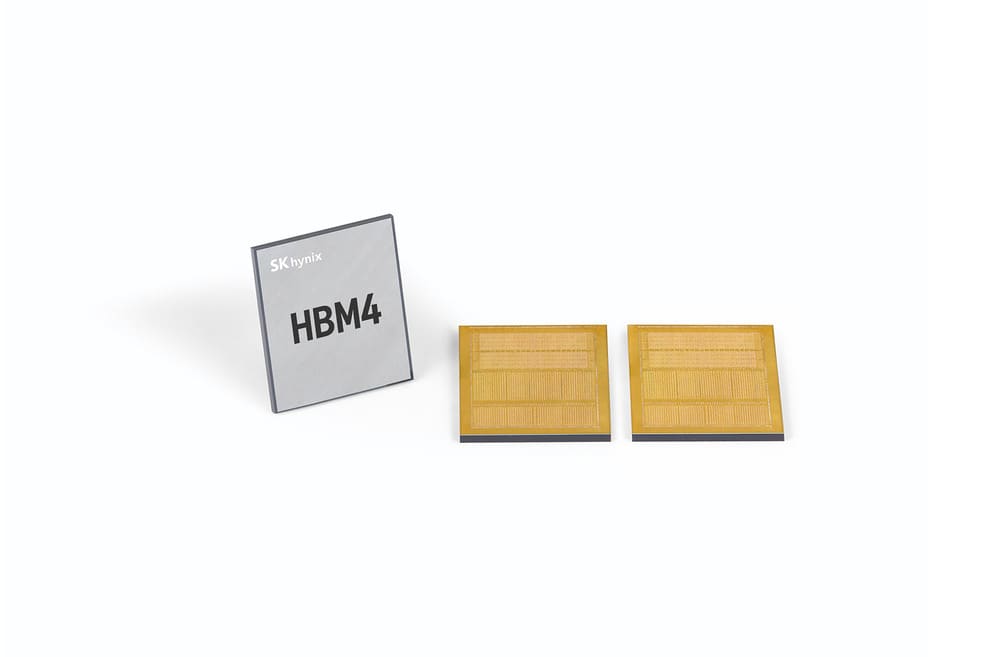
SK Hynix is one of the big winners in the AI cycle thanks to the demand for HBM, a memory essential for GPUs and training/inference accelerators. But selling HBM alone isn’t enough. To ensure this memory works reliably and efficiently alongside high-performance logic chips, the design must consider the packaging type from the outset.
According to published reports, SK Hynix is working with Intel on tests of integrating HBM and logic through substrates with EMIB, Intel’s Embedded Multi-die Interconnect Bridge technology. Unlike solutions based on a large silicon interposer, EMIB uses small embedded bridges within the substrate to connect chips only where high-density links are required. Intel positions this technology as part of its advanced packaging offerings in 2D, 2.5D, and 3D within Intel Foundry.
The technical differences are significant. In a large interposer, costs and complexity tend to increase as the package size grows. EMIB aims to offer greater design flexibility by connecting chiplets via localized bridges. On paper, this allows for better adjustment of each link between dies and avoids the need for a large silicon piece across the entire surface when it’s unnecessary. Intel has also documented evolutions like EMIB 3.5D, combining EMIB with Foveros stacking technology in hybrid designs.
For SK Hynix, exploring EMIB makes sense even if TSMC remains a central partner. The company can better tailor its HBM memories to different packaging architectures, validate materials, study thermal and electrical performance, and reduce dependence on a single industrial pathway. In AI, where product cycles are fierce, being late due to packaging capacity shortages can be as damaging as lacking sufficient memory.
CoWoS Still Dominates, But No Longer Sufficient
TSMC maintains a strong position in advanced packaging. Its CoWoS technology has been key for NVIDIA, AMD, Broadcom, and other AI accelerator or ASIC designers. The problem is that the market has outpaced available capacity. Broadcom has already identified significant supply chain constraints, with TSMC as a bottleneck in advanced manufacturing and AI chip packaging.
This bottleneck has made 2.5D packaging a strategic component. Years ago, much attention was on manufacturing nodes: 7 nm, 5 nm, 3 nm, or 2 nm. Now, for AI, the questions are broader: who can manufacture the logic chip, who can supply HBM, who can package it all, what performance is achieved, what volume is guaranteed, and how long each batch takes to reach customers.
The pressure on CoWoS doesn’t mean TSMC will immediately lose its leadership. The company is investing to increase capacity and benefits from substantial experience, customer relationships, and actual production. But this does open room for alternatives. Intel aims to have EMIB and Foveros as part of that second pathway. Samsung is also strengthening its advanced packaging offerings. Major OSATs like ASE, Amkor, or JCET seek to capture more value. And end customers—from hyperscalers to accelerator manufacturers—want critical production not to depend solely on one supplier.
The potential collaboration between SK Hynix and Intel fits this context. It is not just a technical test; it signals that the industry is beginning to diversify what has been a very concentrated layer. If EMIB demonstrates sufficient performance, cost-effectiveness, reliability, and manufacturing capacity, it could become a partial alternative for certain AI designs.
Intel Seeks a Revival in Advanced Packaging
For Intel, such collaboration could be good news in its attempt to reposition as a foundry. The company has lost ground to TSMC in advanced manufacturing for years but retains valuable technology in packaging, interconnects, and multi-die system design. EMIB isn’t new; Intel has used it in its own products and now seeks to leverage it as a service for external clients.
The market has responded with interest to news about SK Hynix. Financial and tech publications have linked Intel’s stock rebound to perceptions that its foundry and packaging businesses are gaining traction, though it remains to be seen how many of these moves translate into significant contracts and stable output.
Intel’s challenge will be twofold. First, to convince customers it can deliver not just attractive technology but a reliable supply chain. Second, to integrate into an ecosystem where TSMC has been coordinating design, manufacturing, packaging, and collaboration with AI clients for years. In advanced chips, trust is built through performance, delivery timelines, and responsiveness to failures. Having a good packaging architecture alone isn’t sufficient.
There’s also a geopolitical element. The U.S. aims to strengthen its domestic semiconductor capacity—not just wafer fabrication but also advanced assembly. AI has shown that packaging can become a critical point of technological sovereignty. If Intel manages to attract players like SK Hynix to its EMIB ecosystem, it gains relevance in a part of the supply chain that Washington considers increasingly strategic.
Implications for NVIDIA, AMD, and Hyperscalers
Major advanced packaging clients aren’t just traditional chipmakers. NVIDIA depends on such technologies for its accelerators. AMD needs them for its Instinct line and future AI platforms. Companies like Google, Amazon, Microsoft, Meta, and others designing or commissioning their own ASICs also require HBM memory and advanced packaging.
If capacity becomes more diversified, these clients could have more flexibility in planning launches, negotiating capacity, and reducing supply risks. However, not all designs can be seamlessly migrated between technologies—changing from CoWoS to EMIB or vice versa involves fundamental design, validation, thermal, signal, cost, and manufacturing differences.
Thus, the most realistic scenario isn’t rapid replacement of CoWoS but coexistence. TSMC will continue handling the most volume- and maturity-critical designs. Intel might secure projects suited to EMIB regarding design, cost, or availability. Samsung and others will vie for clients seeking alternatives. Meanwhile, SK Hynix, as a HBM supplier, aims to be prepared for all these routes.
The overarching lesson is that the AI chip supply chain is being reshaped. The advantage no longer belongs solely to those designing the most powerful GPU or fabricating the most advanced node. It also goes to those capable of packaging complex chips at scale, with HBM memory, high performance, energy efficiency, and reliable timelines. In this race, packaging has shifted from a secondary phase to a core battlefield in AI hardware.
The collaboration between SK Hynix and Intel remains in early stages, based on available information. But it signifies a real trend: the market cannot indefinitely rely on a single bottleneck. If AI continues growing at the current pace, industry will need more CoWoS, EMIB, Foveros, OSAT capacity, and diverse integration pathways. The future of AI chips isn’t decided just at the fab; it depends on how their components are interconnected.
Frequently Asked Questions
What are SK Hynix and Intel testing?
According to reports from specialized outlets, SK Hynix is testing Intel’s EMIB technology to integrate HBM memory with logic chips using 2.5D packaging.
What is EMIB?
EMIB, Embedded Multi-die Interconnect Bridge, is Intel’s technology that uses small silicon bridges embedded in the substrate to connect chiplets within the same package.
Why is this important for AI?
Because AI accelerators need to integrate high-performance logic chips with HBM memory, a process reliant on advanced packaging technologies like CoWoS, EMIB, or similar solutions.
Can EMIB replace TSMC’s CoWoS?
Not immediately. CoWoS remains dominant in high-volume AI accelerators. EMIB could become an alternative or complement if it demonstrates sufficient performance, reliability, and capacity.
via: zdnet