Memory has become one of the main bottlenecks in Artificial Intelligence. For years, the focus has been on GPUs, accelerators, and large compute clusters, but the actual performance of many systems increasingly depends on how quickly data can be moved. That’s where HBM has become nearly indispensable for training and running advanced models. And it’s also where Intel and SAIMEMORY, a SoftBank subsidiary, want to open an alternative pathway with ZAM, a new high-bandwidth 3D memory architecture.
ZAM, short for Z-Angle Memory, is not yet a commercial product nor a ready-to-deploy memory for hyperscale servers. It is a developing technology with clear ambitions: to deliver more bandwidth, higher density, and lower power consumption than current HBM-based solutions. The technical presentation scheduled at the VLSI Symposium 2026 has provided enough data to start drawing attention—though with cautious optimism. Demonstrating an advanced architecture in a lab is one thing; manufacturing it at volume with competitive costs and industrial reliability is quite another.
What ZAM Proposes Compared to HBM Memory
HBM currently dominates the high-performance memory segment because it allows stacks of DRAM to be placed very close to the processor or accelerator, with an extremely wide interface. It’s a costly and complex solution but fits very well with AI and HPC needs. The just-published HBM4 standard raises the reference bandwidth up to 2 TB/s per stack and offers capacities up to 64 GB per stack in its maximum configurations.
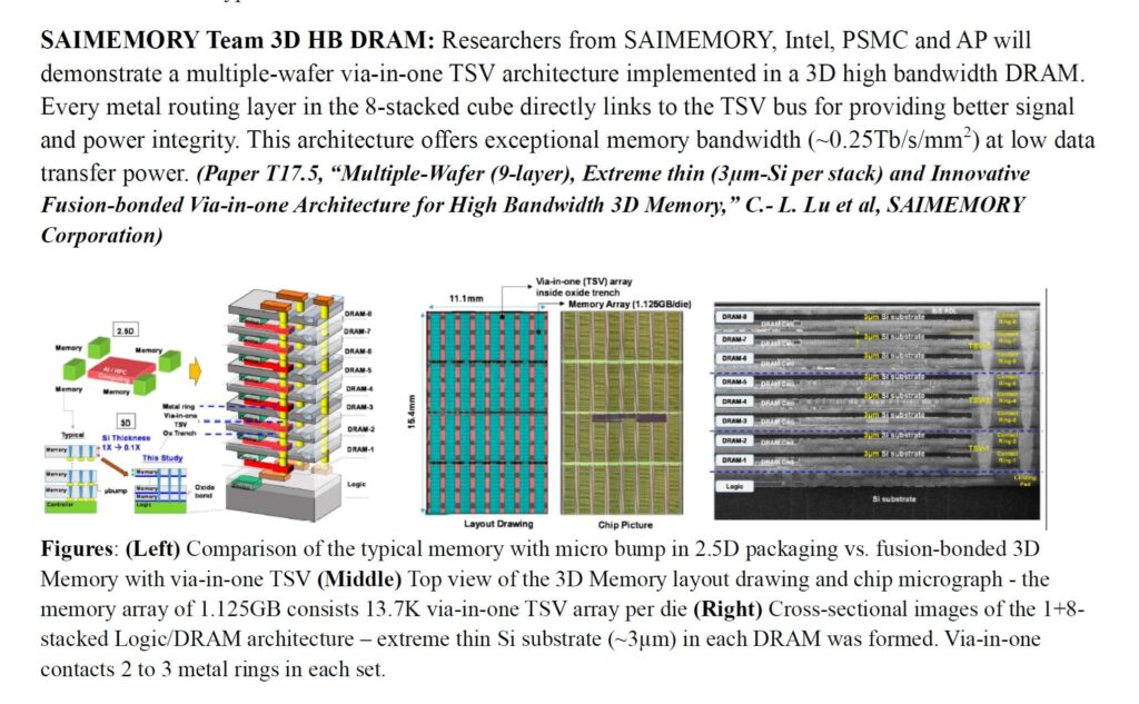
ZAM’s proposal aims to address the same challenge from a different architecture. According to technical materials from the VLSI Symposium, researchers from SAIMEMORY, Intel, PSMC, and AP Memory will introduce a high-bandwidth 3D DRAM memory based on a multi-wafer structure, with a via-in-one TSV architecture and fusion bonding. The design directly connects each routing layer of the eight-layer stacked cube to the TSV bus, aiming to enhance signal integrity and power delivery.
The most striking figure is the bandwidth density: around 0.25 Tb/s/mm² with low power consumption during data transfer. Visual documentation from the presentation also compares common 2.5D packaging with microbumps to a fused 3D memory assembled via via-in-one TSV. The schematic shows a 1+8 architecture, with a base logic layer and eight DRAM layers, using very thin silicon substrates (~3 μm per layer) and a matrix of 13,700 TSVs per die.
Circulating estimates suggest that ZAM could potentially double the bandwidth of HBM4 under specific configurations. It’s important to interpret these comparisons carefully. The consolidated data in the technical summary refer to the architecture’s bandwidth density, not a finalized commercial product specification. For a fair comparison with HBM4 or HBM4E, final capacity, sustained performance, actual power consumption, manufacturing costs, throughput per wafer, and thermal behavior in full accelerators will need to be evaluated.
| Technology | Status | Quoted Bandwidth | Quoted Capacity | Main Challenge |
|---|---|---|---|---|
| HBM4 | Published Standard | Up to 2 TB/s per stack | Up to 64 GB per stack | Cost, supply chain, packaging complexity |
| ZAM | Development and technical demonstration | ~0.25 Tb/s/mm² bandwidth density | Product specifications not finalized | Volume manufacturing and validation in real systems |
An Industry Commitment, Not Just a Technical Presentation
The collaboration between Intel and SAIMEMORY isn’t happening out of nowhere. SoftBank announced in February 2026 that its subsidiary had signed an agreement with Intel to advance the commercialization of ZAM as a next-generation technology aimed at high capacity, high bandwidth, and low power consumption. The company’s plan mentions prototypes during the fiscal year ending March 31, 2028, with commercial deployment possibly in fiscal 2029.
This timeline positions ZAM in a medium-term race. It does not compete directly with current HBM3E nor with early implementations of HBM4, which are expected to arrive sooner. Its natural window appears closer to the next phase of AI infrastructure, where systems will require not just more computation but also more memory per accelerator and less energy per bit transferred.
Intel brings significant expertise in advanced packaging, interconnects, and DRAM bonding technologies. SoftBank, meanwhile, aims to strengthen its position in AI infrastructure from Japan—not just as an investor, but as a driver of foundational technologies. SAIMEMORY was founded in December 2024 to work on next-generation memory chips, aligning with Japan’s strategic goal of regaining influence in advanced semiconductors.
The geopolitical component is also noteworthy. The HBM supply chain is highly concentrated, dominated by a few players—mainly SK hynix, Samsung, and Micron. For companies investing billions in AI data centers, any alternative that can reduce dependence, power consumption, or costs deserves attention. ZAM wouldn’t need to replace the HBM market entirely to be relevant. It could become a viable option in certain accelerator, server, or HPC system designs.
The Critical Test: Manufacturing ZAM at Scale
The most promising aspect of ZAM lies in its vertical architecture. By reducing internal distances and utilizing more direct TSV vias, the technology promises to move data more efficiently, consuming less energy and offering better thermal dissipation compared to some limitations of conventional HBM stacks. This is especially important in data centers, where electrical consumption, cooling, and rack density influence deployment strategies.
However, the history of semiconductors is filled with innovative technologies that took years to reach volume production—or never made it. 3D packaging, fusion bonding, ultra-thin wafers, and the validation of thousands of interconnections per layer are complex tasks. Long-term reliability, defect repair, manufacturing yield, and compatibility with real controllers and accelerators will be as crucial as achieving maximum bandwidth.
There’s also debate about the potential use of mature process nodes for the DRAM layers, especially given PSMC’s involvement. Some interpretations suggest ZAM could leverage less advanced processes than those used for the latest HBM chips, offsetting that difference with architecture and packaging innovations. For now, this remains speculative: the public technical summary confirms the architecture, TSVs, stacking approach, and bandwidth metrics per surface area, but it doesn’t fully define an industrial-grade product.
The realistic expectation is that ZAM opens a new pathway within the AI memory segment, but it won’t immediately displace HBM. HBM already benefits from established standards, a robust supply chain, customer base, ongoing design integrations, and clear presence in products from NVIDIA, AMD, Google, Intel, and other accelerators. ZAM must demonstrate transitioning from a promising architecture to a manufacturable, integrable, and competitive component.
If successful, the impact could be significant. More high-bandwidth alternatives would ease some pressure on the AI accelerator market, enable new chip architectures, and potentially reduce data movement energy costs. Failing that, at least it will have pushed the sector toward more ambitious memory architectures. In either case, the message is clear: the next AI battle will be fought not only in processing cores but also in the memory systems feeding them.
Frequently Asked Questions
What is ZAM?
ZAM, or Z-Angle Memory, is a next-generation 3D memory technology developed by SAIMEMORY with collaboration from Intel. It aims to deliver high bandwidth, high capacity, and lower power consumption in AI and high-performance computing systems.
Will ZAM replace HBM?
It’s too early to say. ZAM aims to compete with HBM in the future, but HBM is already an established standard with solid manufacturers and current product integration. ZAM needs to demonstrate large-scale manufacturing and real-world system deployment.
When could ZAM reach the market?
SoftBank and SAIMEMORY speak of prototypes in fiscal year 2027 (ending March 31, 2028) and potential commercialization in fiscal 2029. This timeline may shift as validation progresses.
Why does this technology matter for Artificial Intelligence?
Advanced models require moving vast volumes of data between memory and accelerators. A memory with higher bandwidth and lower power consumption can improve performance, lower energy costs, and enable denser data center systems.