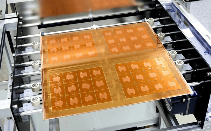
Absolics, the SKC subsidiary specializing in glass substrates for semiconductors, has launched a new project with a U.S.-based communications chip company. According to information published by ETNews, the company has supplied prototypes of “non-embedding” glass substrates for next-generation network semiconductors, and the customer is already conducting reliability tests.
The move is significant because it demonstrates that glass substrates are beginning to move beyond purely experimental stages and are entering projects with specific clients. The chip industry needs new physical platforms to continue enhancing performance, connection density, and energy efficiency—especially in high-frequency applications, advanced networks, Artificial Intelligence, and high-performance computing. In this context, glass is emerging as an alternative to traditional organic substrates, although industrial adoption still faces technical and cost barriers.
Why Glass Is Gaining Interest in Advanced Semiconductors
Substrates are an essential part of semiconductor packaging. They serve as the foundation on which the chip, memory, other components, and the system board are connected. For years, the industry has mainly used organic or advanced plastic materials. These have performed well but are beginning to show limitations as designs require higher density, faster signals, and larger packages.
Glass offers several advantages. It has less deformation, a more stable surface, and better properties for creating fine circuits. This stability is crucial in high-performance chips, where small physical variations can impact connection quality. Additionally, glass can help reduce interconnection lengths, improve efficiency, and enable more compact designs.
Absolics claims that their glass substrates can enhance performance, reduce power consumption, and simplify certain packaging designs for applications like data centers, HPC, and AI. The U.S. Department of Commerce, announcing funding for the company’s Georgia plant, also highlighted that this technology could enable denser interconnections between semiconductors, resulting in faster and more efficient systems.
The project with the U.S. customer targets a different but related use case: next-generation communication and network chips. These semiconductors operate in high-frequency, high-integration environments where substrate quality influences signal integrity, power use, and reliability. As networks for AI, advanced Ethernet, optical interconnects, and low-latency systems expand, packaging materials become increasingly critical for overall performance.
From “Embedding” Substrates to a Faster Path
The most notable aspect of this new project is the type of product involved. Absolics had primarily focused on “embedding” glass substrates, where circuits and passive components can be integrated into the substrate itself. This is an advanced approach with high-density design potential but also involves greater technical complexity.
Now, according to ETNews, the company is expanding its portfolio toward “non-embedding” substrates. This approach does not incorporate circuits and passives within the substrate in the same way, potentially reducing technical difficulties and speeding up time-to-market. Simply put, non-embedding substrates may be a more practical entry point for customers interested in the benefits of glass without yet assuming the full complexity of advanced architectures.
The strategy makes sense. In an emerging technology, the market often adopts a less ambitious, easier-to-qualify solution first—one closer to existing processes and easier to deploy. If non-embedding substrates pass reliability tests, Absolics could move to mass production as early as this year, according to sources cited by the Korean media.
This qualification phase is crucial. In semiconductors, a promising prototype isn’t enough. The material must pass thermal, mechanical, and electrical reliability tests, and demonstrate compatibility with manufacturing, assembly, and packaging processes. Customers require assurances of stable supply, repeatability, and performance before integrating a new substrate into commercial products.
Georgia, CHIPS Act, and the Race for Advanced Packaging
Absolics holds a unique position because its industrial capacity is closely tied to the United States. The company has established a facility in Covington, Georgia, dedicated to advanced glass substrates for packaging. The U.S. Department of Commerce allocated up to $75 million in direct funding through the CHIPS and Science Act to support a 120,000-square-foot plant—about 11,150 square meters—with an anticipated investment of $343 million.
This initiative is part of a broader U.S. strategy to strengthen the supply chain for advanced packaging within the country. For years, much of the semiconductor value chain has been concentrated in Asia, not only in wafer fabrication but also in assembly, testing, and packaging. The rise of AI and chiplet-based designs has elevated packaging to a strategic position comparable to fabrication nodes.
SKC is also bolstering its business. The company appointed Kang Ji-ho as CEO of Absolics in late 2025. Kang brings experience from Intel and SK hynix, and his arrival was presented as a way to accelerate technological competitiveness and operations in glass substrates. Additionally, SKC has announced product advancements with major tech clients and has allocated a significant part of its recent funding to Absolics.
The competition remains stiff. Intel has been researching glass substrates for years and has indicated they could enter production in the latter half of this decade. Other players in the supply chain—including substrate manufacturers, materials, and equipment providers—are also exploring alternatives. The market’s attractiveness is clear: as AI, networking, and HPC chips grow larger and more complex, traditional organic substrates may no longer meet all performance requirements.
Absolics is aiming to stay ahead through a dual approach. On one side, it continues developing embedding substrates for more advanced uses. On the other, it explores non-embedding products that could reach market sooner and address immediate needs. This flexibility is important in a market where clients evolve at different paces.
The collaboration with a U.S. communication chip company does not automatically establish Absolics as the leading supplier of glass for semiconductors. However, it indicates that the technology is progressing to a more concrete stage—demonstrations, qualification, potential production preparations, and customers seeking real improvements over current substrates.
For the industry, the message is clear: chip performance now depends not only on smaller transistors but also on how chips are interconnected, packaged, and powered within increasingly dense systems. The historically inconspicuous substrate is becoming central to the next generation of networks, data centers, and AI developments.
Frequently Asked Questions
What has Absolics announced?
Absolics has supplied prototypes of non-embedding glass substrates to a U.S. communication semiconductor company, which is already performing reliability testing.
What advantages do glass substrates have over organic ones?
They offer greater dimensional stability, less deformation, and better conditions for fine-line circuits, which can benefit high-frequency, high-density, high-performance chips.
What does non-embedding mean in a glass substrate?
It refers to an architecture where circuits and passive components are not integrated within the substrate in the same way as embedding designs. It tends to be less complex and quicker to commercialize.
Where does Absolics manufacture these substrates?
Absolics has a facility in Covington, Georgia, supported by funding from the U.S. CHIPS for America program, specifically for developing advanced glass substrates for packaging.