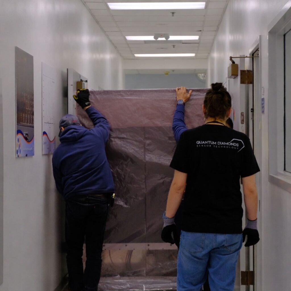
QuantumDiamonds has installed its QDm.1 system at the Integrated Service Technology (iST) facilities in Hsinchu, Taiwan, one of the global hubs of the semiconductor industry. This deployment marks the company’s first installation in Asia and places its quantum microscopy technology using diamonds within a failure analysis laboratory serving top-tier chip manufacturers.
The significance of this news extends beyond initial appearances. As semiconductors progress toward 2.5D and 3D packaging, chiplets, backside power networks, and materials like gallium nitride or silicon carbide, locating electrical faults without damaging the device becomes increasingly challenging. Chips are no longer just smaller; they are denser, more stacked, and far more complex to inspect.
QDm.1 employs Quantum Diamond Microscopy, a technique based on nitrogen-vacancy centers present in diamonds. These controlled defects within the diamond’s crystal lattice enable the measurement of extremely tiny magnetic fields. Since electrical currents generate magnetic fields, the system can reconstruct the current paths inside a chip or encapsulation without cutting, grinding, or layer-by-layer disassembly.
Taiwan: a natural place to validate the technology
The choice of Hsinchu is intentional. The city hosts a vital part of Taiwan’s semiconductor ecosystem, from advanced manufacturing to testing, packaging, materials, design, and failure analysis. Installing QDm.1 at iST allows QuantumDiamonds to position its technology close to clients who encounter the most limitations with traditional inspection methods.
iST is a prominent provider of verification, failure analysis, reliability, and testing services for the chip industry. In this environment, QDm.1 integrates into the failure analysis laboratory to help inspect dense interconnects and complex architectures without damaging the device under test. For manufacturers working with expensive chips, advanced prototypes, or high-value packages, avoiding destructive testing can save time, costs, and samples.
Kevin Berghoff, CEO of QuantumDiamonds, views the installation in Taiwan as validation that quantum sensing is ready for demanding real-world industrial environments. Peter Lemmens, the company’s head for APAC, also highlighted that Hsinchu provides a particularly valuable platform to demonstrate what this technology can offer to the ecosystems of Taiwan, Japan, and Korea.
Just weeks earlier, the company took another significant step by installing a QDm.1 system at Eurofins EAG Laboratories in Sunnyvale, California. With this initial presence in the US and now entry into Taiwan, QuantumDiamonds aims to move beyond European labs toward the two major hubs where much of advanced chip manufacturing and validation occurs.
Why current methods fall short
Failure analysis in semiconductors has traditionally relied on techniques like microscopy, X-ray imaging, thermography, electrical probing, physical slicing, or destructive sample preparation. While still valuable, each generation of chips makes these methods increasingly difficult. Layers multiply, interconnects hide beneath denser structures, and advanced packaging shifts some inspection challenges from silicon alone toward entire system integration.
A recent scientific study applying Quantum Diamond Microscopy to a chip with Integrated Fan-Out Package-on-Package (FO-POP) used in the iPhone illustrates this issue well. Dense redistribution layers and buried interconnects limit the ability of conventional techniques to locate faults without destroying the device. The research validates QDM as a nondestructive method to visualize current paths and identify shorts within complex encapsulations.
This capability becomes crucial in 2.5D and 3D architectures, where multiple chips, memories, and interposers operate together within a single package. It’s also valuable for backside power networks—an approach increasingly adopted by major manufacturers to improve efficiency and density in advanced nodes. When power delivery routes are more complex and less visible, mapping currents nondestructively helps identify defects that previously might have required days of analysis.
The same applies to wide-bandgap materials like GaN and SiC, increasingly used in power electronics, RF, automotive, energy, and communications. Although highly industrially relevant, these materials also pose specific reliability and characterization challenges. A tool capable of observing internal currents non-invasively can be instrumental in detecting hotspots, interconnect faults, or abnormal behaviors in high-value devices.
Europe aims to strengthen its chip metrology capabilities
Founded in 2022 as a spin-out from the Technical University of Munich, QuantumDiamonds’ technology is currently being validated in the US and Asia, but its industrial base remains European. In December 2025, the company announced a €152 million investment plan to establish a manufacturing facility in Munich dedicated to inspecting chips with quantum sensing systems. The project expects to receive tens of millions of euros in public support from the German government and Bavaria under the European Chips Act framework.
This is significant for Europe. The region seeks to reinforce its position in the semiconductor supply chain but cannot compete solely with wafer fabrication plants. It also needs equipment, metrology, materials, design software, advanced packaging, and inspection tools. ASML has demonstrated that a European company can become an essential part of the global industry by occupying a critical segment in the chain. QuantumDiamonds aims for something still emerging and to be proven but shares a similar trajectory: addressing a technical bottleneck affecting all advanced manufacturers.
The installation of QDm.1 in Taiwan does not automatically make the German company an essential provider. Adoption of new semiconductor tools is slow, demanding, and depends on comparative testing, technical support, workflow integration, and industrial repeatability. However, it shows that quantum sensing is beginning to have real-world applications outside academic labs.
For chip manufacturers, the potential benefit is clear: detecting faults earlier, with less sample destruction, and more insight into what happens inside the package. In an industry where manufacturing yield and diagnostic time can mean millions of euros in difference, reducing uncertainty in failure analysis has direct value.
The race for AI, chiplets, and advanced packaging not only requires better GPUs or smaller process nodes but also tools capable of verifying these architectures function as intended. QuantumDiamonds is working to prove that diamonds used as quantum sensors can become a new window into the inner workings of more complex chips.
Frequently Asked Questions
What has QuantumDiamonds installed in Taiwan?
QuantumDiamonds has set up its QDm.1 system at iST’s failure analysis laboratory in Hsinchu. This marks its first installation in Asia.
What is Quantum Diamond Microscopy?
It’s an inspection technique using nitrogen-vacancy centers in diamonds to measure magnetic fields and reconstruct current paths within chips and packages nondestructively.
Why is this important for 2.5D and 3D chips?
Because these chips feature dense interconnects, buried layers, and structures that are difficult to inspect with traditional methods. Nondestructive inspection can speed up failure analysis significantly.
Is QuantumDiamonds a European company?
Yes. It is a German company originating from the Technical University of Munich, with plans to establish a €152 million manufacturing facility in Munich.