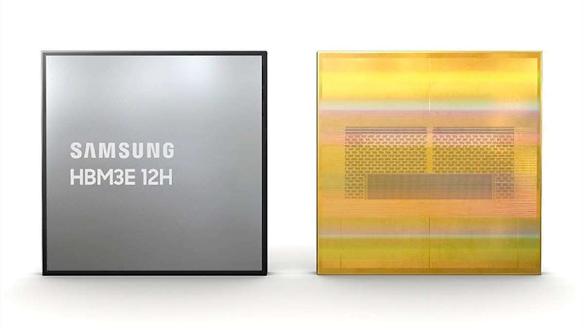
Samsung Foundry may have reached a significant milestone in its industrial recovery. According to a report published by Seoul Economic Daily, Samsung Electronics’ contract chip manufacturing division has achieved over 80% yield in its 4-nanometer process, a level the South Korean media describes as entering the “mature process” phase. Samsung has not officially confirmed this figure, but if validated, it would shift the narrative that has long been dominated by doubts regarding its yields compared to TSMC.
Manufacturing yield measures how many functional chips are produced from a wafer. In advanced semiconductors, it’s not a mere accounting detail: it impacts costs, margins, delivery capacity, and customer trust. A low-yield process requires fabricating more wafers to get the same number of usable chips. Once a process surpasses certain thresholds, it becomes more attractive for companies needing to produce AI accelerators, custom processors, or high-volume components.
Samsung’s 4 nm Seeks a Second Chance
Samsung began producing its 4 nm nodes several years ago, but its foundry business has been under pressure. TSMC remains the clear market leader, while Samsung has tried to convince clients that its advanced processes can deliver sufficient performance, efficiency, and capacity. The reported improvement to over 80% yield at 4 nm doesn’t automatically make Samsung an equivalent alternative to TSMC across all segments, but it does strengthen its position in a node that is no longer experimental.
This news comes at a particularly favorable time for foundries capable of producing AI chips. Demand isn’t just from massive training GPUs but also from inference accelerators, specialized processors, ASICs, base dies for HBM memory, and custom designs for data centers. In this market, a mature 4 nm node can be highly competitive if it offers good cost efficiency, available capacity, and a reliable path to volume production.
Seoul Economic Daily reports that the yield improvement is attracting orders from companies like Groq, IBM, Baidu, Ambarella, and Faraday, as well as South Korean AI chip companies such as Rebellions and FuriosaAI. Although this should be interpreted as industry insight rather than a confirmed list from Samsung, it aligns with a clear trend: many firms are seeking alternative manufacturing options outside TSMC to reduce dependence and secure capacity.
| Key Report Insights | Implications for Samsung |
|---|---|
| Yield above 80% at 4 nm | Fewer defective chips and better cost per unit |
| Considered a mature process | Increased confidence for high-volume customers |
| Orders linked to AI | Entry into a high-demand market |
| Groq as a key client | Strengthening inference accelerators capabilities |
| Base die of HBM4 | Potential synergy between foundry and memory manufacturing |
| Pressure on TSMC | Samsung gains commercial leverage, though not fully rivaling TSMC’s leadership |
Groq, NVIDIA, and the Role of Inference
Groq’s case is among the most notable. In 2023, the company announced it had selected Samsung Foundry to manufacture its next-generation LPU (Language Processing Unit) using the SF4X 4 nm process. This collaboration placed Samsung within an emerging category: chips specifically designed to accelerate language inference models with low latency and high efficiency.
The relationship has gained visibility within the NVIDIA ecosystem. NVIDIA describes the Groq 3 LPU as a key inference component for its Vera Rubin platform, integrated into LPX racks with 256 interconnected LPUs. NVIDIA’s documentation indicates each LPU has 500 MB of SRAM, 150 TB/s SRAM bandwidth, and 2.5 TB/s scale-up bandwidth.
This doesn’t make Samsung a supplier of NVIDIA’s GPUs, but it does position Samsung close to a critical segment of AI deployment: inference. As models are used continuously in agents, assistants, search, code generation, and enterprise applications, the cost of serving responses becomes just as vital as training. Specialized low-latency accelerators may become more prominent, and Samsung aims to be a manufacturing partner in this space.
For Samsung Foundry, producing chips like this holds strategic value. It’s not just about volume but also credibility. If a company involved in one of the most visible inference deployments trusts its 4 nm node, the message to the market differs from past years of performance issues, delays, or lost clients.
HBM4 and the Advantage of Integrating Memory and Foundry under One Roof
Another notable point from the Korean report is the connection to HBM4 memory. Samsung isn’t just a foundry; it’s also one of the world’s leading memory manufacturers. Seoul Economic Daily states that its foundry division would produce the base die for HBM4—the logical component beneath high-bandwidth memory stacks.
This integration could be significant. HBM memory has become one of the most scarce and valuable components in AI infrastructure. Modern accelerators require enormous bandwidth, and the base die has become increasingly sophisticated. If Samsung can better coordinate foundry, memory, advanced packaging, and AI customers, it could recapture ground against SK Hynix in HBM and against TSMC in other parts of the ecosystem.
Yet, this advantage isn’t assured. Samsung has faced challenges convincing the market that it can compete at the highest levels across all fronts simultaneously. Nonetheless, few manufacturers combine such broad capabilities in memory, logic, packaging, and industrial capacity. In an era where AI chips are complete systems rather than just isolated processors, this level of integration remains a compelling selling point.
The Ongoing Race with TSMC
The progress at 4 nm doesn’t close the gap with TSMC’s most advanced nodes. The battle over 2 nm and subsequent generations will continue to shape market perception. It remains to be seen whether Samsung can sustain high yields in continuous production, meet deadlines, attract large-volume designs, and improve margins within its foundry division, which has faced headwinds over multiple cycles.
Nevertheless, recovering a mature node can prove as crucial as winning headlines with the latest process. Many AI chips do not require the most advanced node if their design is well-optimized and unit costs are competitive. In inference, automotive, enterprise ASICs, networking chips, or specialized accelerators, a stable 4 nm process can be highly attractive.
For customers, Samsung’s improvements are also positive. The market needs more advanced capacity and options. Over-reliance on a single manufacturer introduces risks related to pricing, supply, and geopolitics. If Samsung becomes a more reliable alternative at 4 nm, companies like Groq, IBM, Baidu, and emerging AI designers could have greater negotiating power, scaling, and diversification choices.
The critical question is whether this momentary advance signals a trend. Achieving over 80% yield is a strong indicator, but the market will evaluate Samsung’s consistency. Foundry is a trust-based business: it’s not enough to produce well in one generation—quality, roadmap stability, capacity, and support need to be maintained over years.
Samsung needs that confidence to secure high-value orders again. AI offers a clear window of opportunity. If 4 nm matures, HBM4 advances, and inference customers scale, the South Korean company could recapture some lost ground—not because TSMC will stop leading tomorrow, but because the industry can no longer afford to depend solely on one entry point for the next wave of AI chips.
Frequently Asked Questions
What does an 80% yield at 4 nm mean for Samsung?
It means that, according to the report, over 80% of chips produced with that process are functional. A high yield reduces costs and enhances the commercial viability of the node.
Has Samsung officially confirmed this figure?
No official confirmation from Samsung has been reported. The figure originates from Seoul Economic Daily and should be considered industry data sourced from a South Korean media outlet.
What is the relationship between Groq and Samsung Foundry?
Groq announced in 2023 that it would manufacture its next-generation LPU (Language Processing Unit) using Samsung’s SF4X 4 nm process. Its inference chips are also part of NVIDIA’s Vera Rubin ecosystem.
Does this mean Samsung is now competing on equal footing with TSMC?
Not necessarily. While the improved 4 nm yield solidifies Samsung’s position in a mature node segment, TSMC continues to lead in advanced processes like 2 nm, and the race for next-generation nodes remains open.
via: wccftech