Intel Foundry has focused on one of the most sensitive and strategic markets in the semiconductor industry: aerospace, defense, and government systems. In a new technical document and contextual overview authored by Tao Zhou, Intel’s chief engineer, the company highlights that many critical platforms still rely on outdated microelectronics, creating an increasing gap between current operational demands and the actual capabilities of deployed systems. Intel’s proposal involves a combination of advanced nodes, chiplets, heterogeneous packaging, and secure manufacturing in the United States.
This is not a finalized product announcement or a specific contract with the U.S. Department of Defense, but rather a clear move to position Intel Foundry as a modernization partner for workloads where compute density, secure communications, AI readiness, and the size, weight, power, and cost (SWaP-C) constraints are paramount. Intel presents this combination as a way to modernize mission-critical systems without relying on a single technological piece, but rather a broader stack that includes process, encapsulation, assembly, and testing.
Intel 18A aims to be the centerpiece of this modernization
Intel’s core message centers on the Intel 18A family. The company notes that this node incorporates two of its major technological bets: RibbonFET, its implementation of gate-all-around transistors, and PowerVia, its back-side power delivery architecture. According to Intel Foundry’s official documentation, 18A is already considered ready for customer projects and is a significant asset for advanced designs manufactured in North America.
Addressing the aerospace and defense sector, Intel claims that compared to Intel 16, the 18A node can deliver up to twice the performance at the same power, five times lower power at equivalent performance, and ten times greater density. These figures are based on Intel’s internal analyses and should be viewed as manufacturer’s references rather than independently verified comparisons. Nonetheless, they support Intel’s thesis that the new generation of nodes isn’t just for commercial CPUs or accelerators but also for power-constrained, space-limited, and rugged platforms.
Intel further introduces two variants with specific relevance to this market. Intel 18A-P is optimized for a balance of high-speed logic and ultralow power consumption, while Intel 18A-PT, still in development, would feature a base die with backside power delivery through TSVs and hybrid bonding, easing the development of high-performance 3DIC architectures. This latter variant signals an emphasis on more complex heterogeneous systems where stacking and interconnecting multiple specialized dies are crucial, not just relying on the main logic node.
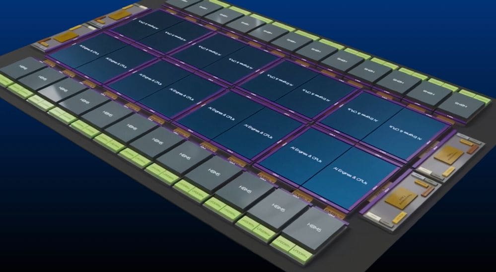
Packaging as a strategic element rather than an afterthought
The second major pillar in Intel’s argument is advanced packaging. Intel Foundry emphasizes that meeting SWaP-C and performance goals requires more than improved dies; integrating multiple chiplets with high bandwidth and low latency is essential. Technologies like EMIB 2.5D, Foveros, Foveros Direct 3D, and EMIB-T are highlighted—this last designed for very large formats with enhanced power and signal delivery through TSVs.
This approach aligns with Intel Foundry’s overall strategy, which aims to be a leader in differentiated packaging. The company’s website states a target of reaching 1 trillion transistors per package by 2030. In defense applications, heterogeneous packaging isn’t just about fitting more compute into less space but also about enabling modular updates and reducing reliance on monolithic, rigid designs.
Additionally, Intel introduces Intel Foundry ASAT, its advanced assembly and test offering. Described as a layer tailored for strategic systems, it can handle everything from individual dies to complete system validation. In sectors like defense and government, this part of the process is nearly as vital as the node technology, as traceability, testing, and assembly integrity contribute significantly to the product’s industrial and regulatory value.
Thermal reliability, RF, and trusted manufacturing in the U.S.
Intel’s document also addresses thermal management, increasingly critical in high-performance systems. The company claims to have developed integrated heat spreaders optimized for liquid cooling and reports, based on preliminary internal evaluations, that these solutions could offer more than three times the thermal efficiency compared to reference air-cooled designs. While preliminary, these results underscore the importance of cooling systems in next-generation designs where power density is higher and thermal management is integral to performance.
In the analog and RF domain, Intel asserts that 18A combines dense, efficient digital logic with high-speed analog capabilities suitable for direct RF sampling. This makes it attractive for advanced radar and secure, high-bandwidth communications. Intel also mentions collaboration with UMC on a 12 nm process aimed at RF transceivers, satellites, and cost-sensitive electronics, but with a notable caveat: this joint node is not eligible for U.S. defense applications, as explicitly indicated in the documentation’s notes.
The political and industrial implications are also clear. Intel links its offerings to U.S. government programs like RAMP-C and SHIP, designed to provide the defense ecosystem access to advanced process and packaging technologies. In January 2025, Intel explained that RAMP-C enables defense industry customers to leverage Intel 18A and advanced packaging for prototypes and high-volume manufacturing. The SHIP program, defined by Qorvo and the DoD, aims to secure sustained access to state-of-the-art heterogeneous packaging via commercial manufacturing streams. Furthermore, in 2024, Intel received up to $3 billion in federal funding for its Secure Enclave initiative, which the company positions as part of its commitment to reliable domestic manufacturing.
Overall, Intel aims to craft a compelling narrative: that it can supply not only advanced nodes but also a comprehensive, U.S.-based modernization pathway for sensitive systems. The key uncertainty remains how much of this promise will translate into concrete programs, deployed designs, and sustained contracts. In defense, technology matters, but industrial execution and institutional trust weigh even more heavily.
Frequently Asked Questions
What exactly has Intel presented for the aerospace and defense sector?
Intel has not announced a finalized new product but rather a modernization proposal based on Intel 18A, chiplets, advanced packaging, assembly, and testing, targeted at aerospace, defense, and government systems.
What role does Intel 18A play in this strategy?
It forms the core technology platform. Intel positions it as its advanced node for clients, featuring RibbonFET and PowerVia, with significant improvements in density, efficiency, and performance over Intel 16 in SWaP-C constrained workloads.
Which U.S. government programs support this direction?
Intel ties its offerings to RAMP-C and SHIP, and has received up to $3 billion under the Secure Enclave program aimed at reinforcing trusted manufacturing of advanced semiconductors for the U.S. government.
Is the 12 nm joint node with UMC suitable for U.S. military applications?
No. Intel’s own documentation states that this 12 nm process with UMC is not eligible for U.S. defense applications, though it is intended for RF, satellites, and cost-sensitive electronics.
via: community.intel