The back-end semiconductor equipment business is starting to occupy a much more prominent spot in the global chip industry. A market report from The Business Research Company estimates this market will exceed $34 billion by 2030, with Asia-Pacific as the dominant region and China as the primary country by projected volume. These figures should be viewed with caution, as they are based on private market studies rather than audited official statistics, but they reflect a trend consistent with the sector’s current moment: assembly, packaging, and final testing have become a critical piece in delivering increasingly complex chips.
The underlying reason isn’t just about manufacturing more but about manufacturing better. The surge in demand driven by Artificial Intelligence, HBM memory, high-performance computing, and chiplet-based designs has pushed the entire value chain to pay much closer attention to the final phase of production. SEMI forecasts that the back-end segment will maintain growth in 2026, with testing rising by 12.0% and assembly and packaging by 9.2%, fueled by the increasing complexity of architectures and the performance demands of AI and HBM chips.
From Classic Encapsulation to Advanced Packaging
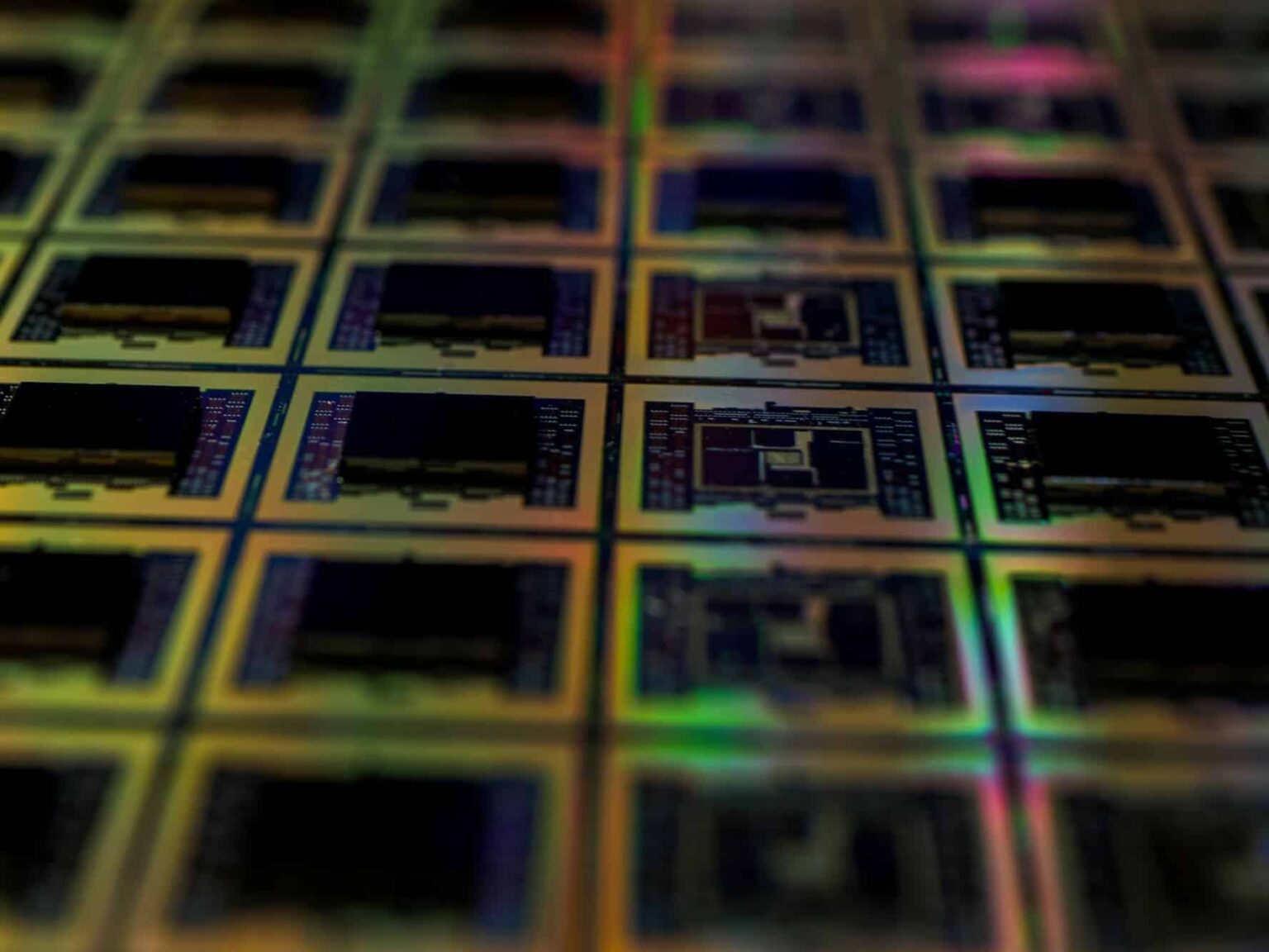
When discussing back-end, it generally refers to the final stages of semiconductor manufacturing: die preparation, die bonding, wire bonding, encapsulation, assembly, and testing. This is not a minor or purely logistical phase. It plays a crucial role in the component’s reliability, thermal management, power consumption, integration with memory or advanced substrates, and ultimately its real-world performance once launched. Commercial descriptions of the market identify die bonding, wire bonding, packaging, and testing as major segments within this industry.
This shift towards greater industrial significance is clearly reflected in the strategies of major manufacturers. TSMC has been emphasizing for years that value no longer resides solely in the fabrication node but also in integrating multiple chips into systems. Their 3DFabric platform combines technologies like SoIC, CoWoS, and InFO, framing them as a blend of front-end and back-end technologies aimed at solving heterogeneous integration challenges and scaling to volume. In other words, packaging has moved beyond a final step to become a key competitive factor.
This momentum is evident in the financial results of several specialized companies. ASMPT reported revenues of $532.1 million in advanced packaging in 2025—up 30.2% year-over-year—driven by robust demand for its TCB solutions. Besi, one of the most closely watched names in this niche, raised its long-term financial targets in 2025, citing increased demand for advanced packaging solutions for logic and memory. Teradyne closed Q4 2025 with $883 million in Semiconductor Test within total revenues of $1.083 billion, supported by AI-related demand in computing, networking, and memory. These are not isolated moves—they demonstrate that the chip bottleneck is no longer only about wafers but also about how chips are packaged and validated.
Asia Leads Spending, China Continues to Set the Pace
The market report released this week indicates that Asia-Pacific could reach $17 billion in 2030 in this sector, while China alone might account for around $10 billion. This aligns with the actual geographic distribution of the industry: much of the assembly, testing, and packaging capacity is concentrated in Asia, where many leading OSATs and large manufacturers with significant industrial strength operate. It’s also where the combined effects of government support, technological self-sufficiency pressures, and capacity expansion are most pronounced.
SEMI’s data point in the same direction, although they don’t measure exactly the same subsegments. The association anticipates that China, Taiwan, and South Korea will continue to be the leading destinations for semiconductor equipment spending through 2027. In Taiwan, much of this activity remains tied to cutting-edge capacities related to AI and high-performance computing. In China, the market’s weight remains substantial despite expected moderation following years of aggressive investment. This combination helps explain why back-end is gaining so much prominence: it’s not just about building factories, but also about having the machinery capable of assembling, encapsulating, and testing increasingly demanding chips.
A Growing Market with Caution on Forecasts
Nevertheless, the story shouldn’t be read as if there’s a single unquestionable figure. Another market study from ResearchAndMarkets presents a somewhat more conservative outlook: $23.54 billion in 2026 and $32.76 billion in 2030. The difference from the $34 billion threshold does not change the overall trend, but it underscores that different reports work with distinct methodologies, definitions, and scopes. In such specialized markets, even a small variation in what each firm counts as “back-end equipment” can imply billions on paper.
Beyond exact figures, the key message is the industrial significance. The final phase of chip production can no longer be regarded as a secondary activity or low-value addition. The expansion of AI, advanced memory, chiplets, and 2.5D and 3D packaging is channeling investment toward machines that assemble, encapsulate, connect, and test these components. Although the back-end market will remain smaller than the front-end equipment sector, it will become increasingly strategic in determining which companies can scale production, improve performance, and capture value in the new semiconductor race.
Frequently Asked Questions
What does back-end mean in chip manufacturing?
It refers to the final stages of semiconductor fabrication, where the chip is diced, mounted on substrates or encapsulated, connected, protected, and tested before commercial release. It includes die bonding, wire bonding, packaging, and testing equipment.
Why is advanced packaging so important in 2026?
Because AI chips, HBM, and high-performance computing require integrating multiple dies, memory, and advanced substrates with higher density, better thermal management, and wider bandwidth. TSMC, for example, highlights its CoWoS, InFO, and SoIC technologies as central to this evolution.
Which companies are most benefiting from the surge in semiconductor back-end?
Leading firms include assembly, packaging, and testing equipment manufacturers like ASMPT, Besi, and Teradyne. Their recent results show a strong growth in demand for solutions related to advanced packaging and AI chip testing.
Will Asia continue to lead this market in the coming years?
All indications suggest yes. Market reports position Asia-Pacific as the dominant region, with SEMI projecting China, Taiwan, and South Korea as the main spenders on semiconductor equipment in the foreseeable future.
via: semiconductors news