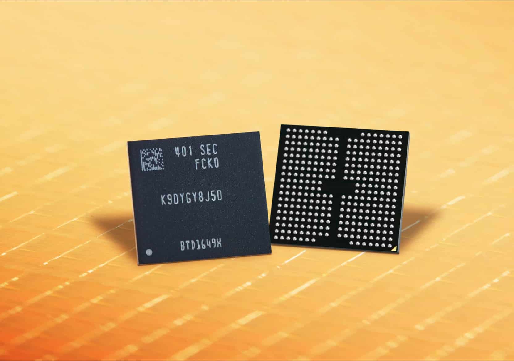
The race for the infrastructure that will support the next wave of Artificial Intelligence is no longer limited to GPUs or HBM memory. It’s also starting to take place in storage, where Samsung and NVIDIA are making an interesting move. There’s no evidence of a traditional commercial announcement nor of NVIDIA manufacturing NAND memory, but there is a real research collaboration between both companies and Georgia Tech to speed up the development of ferroelectric-material-based NAND memory through AI models and accelerated computing.
This nuance is important because it helps avoid jumping to easy headlines. What can be confidently stated today is that Samsung is working on new, ultra-low-power NAND architectures, and researchers from Samsung Semiconductor Research, NVIDIA, and Georgia Tech have presented a Physics-Informed Neural Operator (PINO) model capable of drastically speeding up the analysis of these types of devices. The scientific basis has been published, and the industrial context points to broader collaboration, but there’s no official product line or finalized commercial roadmap for an “NVIDIA NAND” yet.
What is truly known about this collaboration
The most solid piece of this story is the scientific research. On March 6, a study titled “Physics-informed AI Accelerated Retention Analysis of Ferroelectric Vertical NAND: From Day-Scale TCAD to Second-Scale Surrogate Model” was published on arXiv, authored by researchers from Samsung, NVIDIA, Georgia Tech, and others. The paper describes how a PINO model can analyze the behavior of a ferroelectric vertical NAND with an acceleration over 10,000 times compared to traditional TCAD simulations, while maintaining physical consistency in the results.
This figure of 10,000 times should not be interpreted as “the memory will be 10,000 times faster,” because it doesn’t refer to the final performance of a commercial SSD or chip. Instead, it indicates the speed-up in simulation and analysis during R&D. Rather than spending hours exploring parameter combinations, materials, and structures, teams can get predictions in seconds and test many more variants in less time. In an industry where each memory upgrade can take years of modeling, validation, and pilot production, such acceleration could significantly shorten development cycles.
The second key piece comes from Samsung. In November 2025, Samsung Semiconductor announced that a team from the Samsung Advanced Institute of Technology (SAIT) had published in Nature a paper on ferroelectric transistors for low-power NAND memory. This study claims the proposed architecture can reduce energy consumption by up to 96% during string-level operations compared to conventional approaches, while maintaining multi-cell storage capacities comparable to current NAND. That 96% figure is supported by technical and official sources, but it should be understood as an experimental research result, not an immediate product promise.
Why ferroelectric NAND is so relevant in the AI era
Traditional NAND remains essential for SSDs, enterprise storage, and AI service systems, but it faces increasingly tough physical limits. As layers and densities increase, electrical control becomes harder, power consumption rises, and the margin for scalability without penalties shrinks. The ferroelectric approach aims to address this problem by replacing some of the charge-based logic with structures capable of storing electrical states more efficiently.
This is where NVIDIA’s industrial logic comes into play. The company doesn’t need to become a NAND manufacturer to have a stake in this technology. Their AI systems, cloud partners, and the entire ecosystem of accelerators demand faster, denser, and more efficient storage. As AI drives the demand for memory and data center storage, participating in tools that accelerate the design of next-generation NAND also strengthens NVIDIA’s position along the value chain. Reuters has also noted that Samsung and NVIDIA have deepened their relationship in other areas, such as HBM4 and the creation of a semiconductor plant powered by over 50,000 NVIDIA GPUs.
For Samsung, the motivation is equally clear. It remains the world’s leading NAND flash supplier by revenue, holding roughly a 32% market share according to Counterpoint Research, in a market that’s benefiting again from AI infrastructure and the growth of server storage. Maintaining that position will require more than increasing production; Samsung needs to find the next major NAND architecture before competitors like SK Hynix/Solidigm, Kioxia, or Micron do.
The 1,000-layer goal remains aspirational
An aspect generating a lot of buzz is the supposed leap toward 1,000-layer NAND memories. It’s important to differentiate between confirmed information and speculation. Korean outlets like Sedaily and analyses from TrendForce present ferroelectric NAND as a promising pathway toward that threshold, but neither the Nature article nor the arXiv preprint claim that Samsung has already achieved this goal or that there’s an industrial timeline to reach it. For now, it’s more accurate to describe this as a plausible technological direction rather than an imminent product.
Nonetheless, the significance of this news is not diminished by that nuance. If anything, the most interesting aspect is that AI is starting to become directly involved in the actual design process of advanced memory. Whereas until now the debate centered around using AI for generating text, code, or images, this case introduces a much more strategic layer: employing AI to accelerate physics modeling, simulation, and engineering of components that will underpin future data centers.
In other words, the AI race isn’t just about training bigger models anymore. It’s also about building memories, chips, and systems that can support them with lower power, higher density, and shorter development cycles. Samsung brings memory expertise; NVIDIA contributes computational infrastructure and AI muscle. The current result is not a market-ready product but an R&D collaboration with much deeper implications than it appears at first glance.
Frequently Asked Questions
Have Samsung and NVIDIA announced a new NAND memory product?
No. What is publicly supported is a research collaboration on ferroelectric NAND and an AI model to accelerate its analysis. No jointly developed NAND product has been officially announced or presented yet.
What is ferroelectric NAND?
It’s a research area exploring flash memory that uses ferroelectric materials to improve efficiency and scalability over conventional NAND. Samsung published experimental results in Nature indicating much lower energy consumption in string-level operations.
What does it mean that AI accelerates analysis by 10,000 times?
It doesn’t mean the final chip will be 10,000 times faster. Rather, the PINO model can speed up simulation and modeling work compared to traditional TCAD tools, reducing analysis times from days to seconds.
Is the goal of 1,000-layer NAND real?
It’s a technological direction cited by Asian media and analysts like TrendForce, but it’s not an officially announced near-term target by Samsung in technical documents. For now, it should be considered a future aspiration, not a confirmed specification.