Although they are often overshadowed by wafers, nodes, or the race for artificial intelligence, lead frames remain a critical component in the semiconductor industry: without them, millions of chips couldn’t “talk” to the outside world. And, according to the latest forecasts published in a sector report, their global market is accelerating amid full vehicle electrification and miniaturization pushing the limits once again.
Estimates place the semiconductor lead frames market at $3.83 billion in 2025 and project an increase to $4.11 billion in 2026, representing a compound annual growth rate (CAGR) of 7.5%. The same source anticipates the market could reach $5.5 billion by 2030, with a CAGR of 7.6% over that period.
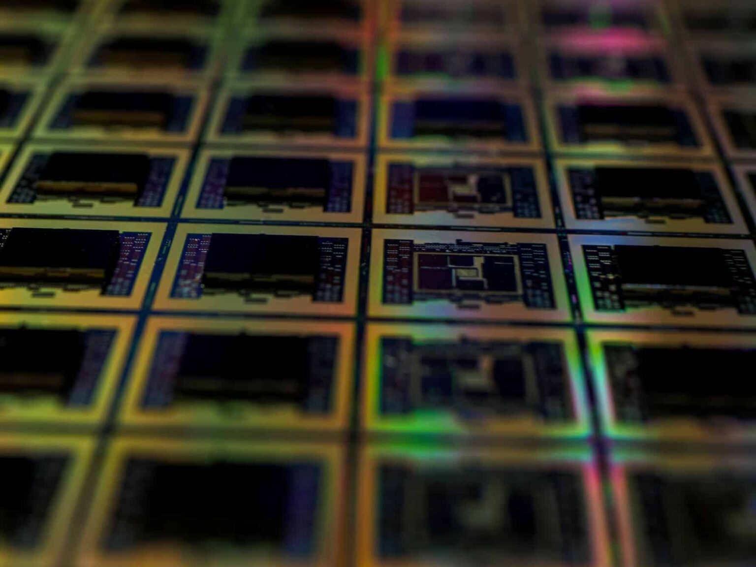
What is a lead frame and why does it matter (more than it seems)
A lead frame is essentially the physical and electrical interface between the chip (the die) and external circuitry, such as a PCB. It provides electrical connectivity, mechanical support, and aids in thermal management within the package: the metal “chassis” that makes the semiconductor a usable component at an industrial scale.
Here, various families coexist: processes based on stamping and etching/chemical attack, along with materials ranging from Copper and copper alloys to options like iron-nickel. The choice is not trivial: it affects tolerances, pin density, heat dissipation, and reliability.
Electric vehicle push for a big entrance
The most repeated growth driver in analysis is the expansion of electric vehicles. It’s not just more “battery-powered” cars: each EV multiplies the demand for power, control, and sensor semiconductors, and these chips require robust packages.
A figure that helps put this phenomenon into perspective: in the United States, 1.4 million new electric vehicles were registered in 2023, more than a 40% increase over 2022, according to the Global EV Outlook 2024 report by the International Energy Agency.
As the vehicle becomes an electronic platform (inverters, converters, battery management, ADAS), the package ceases to be just a detail and becomes a requirement: thermal resistance, temperature cycles, vibrations, and lifespan.
Miniaturization and density: the “fine-pitch” returns to center stage
Beyond EVs, the report highlights clear technical trends: higher density and fine-pitch, growth of copper/copper alloy use, increased presence in automotive packaging, improvements in heat dissipation, and greater traction of etching in miniaturized integrated circuits.
Practically, this means competing on two fronts simultaneously:
- Scale and cost (high volume in consumer electronics and industrial applications).
- Quality and reliability (automotive and telecom, where margins depend on performance and traceability).
Defect control: when a microscopic thread determines performance
A particularly revealing point is how inspection of wire bonding (the wires connecting the chip to the lead frame in many packages) is changing. If pitch narrows and volumes increase, defect detection shifts from “quality control” to business continuity assurance.
In that regard, advances like Keysight’s Electrical Structural Tester (EST), designed to detect wire bond defects (e.g., wire sag, near shorts, or “errant” wires), with a high-throughput approach, are cited.
Geography: North America leads today, but Asia is accelerating
Regionally, the same source places North America as the largest region in 2025, while Asia-Pacific will experience the fastest growth in the coming years.
This reflects a near-complete picture of the global supply chain: North America concentrates much of the design work, high-value segments, and some advanced demand; Asia-Pacific remains the main manufacturing hub (assembly, packaging, volume), alongside industrial policies and capacity expansion.
The uncomfortable variable: trade, tariffs, and a “dynamic” outlook
One nuance the market cannot ignore: forecasts are conditioned by an environment of trade tensions and tariffs that could alter costs, supply routes, and investment decisions. The report itself warns that its outlook is affected by these rapid changes and that forecasts and quantified impacts will be adjusted as the situation evolves.
In other words: growth is real, but the picture could shift if the rules of the game change (materials, logistics, origin requirements, subsidies, etc.).
Frequently Asked Questions
What is the difference between a stamped lead frame and an etched one?
Stamping generally prioritizes productivity and lower cost at high volume; etching allows for finer, more precise geometries, useful when the package requires higher density and tighter tolerances.
Why does electric vehicle demand significantly increase lead frame requirements?
Because an EV contains more power and control electronics, and those semiconductors need reliable packages with good thermal management and robust interconnections. The growth in EV registrations directly indicates increased downstream demand.
What role does copper play in this evolution?
Adoption of copper and copper alloys in lead frames is increasing due to their electrical and thermal advantages, especially important in power applications and designs where heat dissipation and reliability are critical.
Why is wire bonding defect detection so important?
Because shrinking sizes and increasing volumes mean small defects in interconnection wires can cause failures and losses. The industry is pushing for more advanced testing and inspection solutions to ensure integrity at scale.