A new American startup aims to place photonics — light-based computing — at the forefront of the debate about the future of hardware for Artificial Intelligence. Neurophos, based in Austin (Texas), has announced a Series A funding round of $110 million (with a total of $118 million including previous funding) to accelerate the development of its Optical Processing Units (OPUs), a family of accelerators oriented toward AI inference that, according to the company, strive to deliver performance and efficiency leaps impossible to sustain with conventional silicon.
The core thesis behind the investment is clear: the industry is encountering physical and operational limits. The “power wall” is no longer just a metaphor; it’s a real barrier in data centers, driven by electrical availability, cooling, and overall cost. In this context, it’s not surprising that giants and startups are exploring alternative routes, from silicon photonics for interconnects to new computing paradigms. Reuters, for example, has been tracking how photonics is gaining importance in networks and advanced packaging for AI infrastructures, precisely because of its potential for data movement efficiency.
What is an OPU and why does it matter for AI?
Unlike a traditional GPU, where each operation involves electrical switching, an OPU aims to execute critical AI operations (especially matrix multiplications) by leveraging physical properties of light. Practically, Neurophos claims that its architecture integrates more than a million optical processing elements on a single chip, with a key advancement based on micrometric optical modulators made from metamaterials, achieving miniaturization that could enable scaling photonic matrices to densities viable for product deployment.
The promise is compelling for operational reasons: in many photonic approaches, “computation” can be relatively energy-efficient once the signal is in the optical domain. The high costs are shifted to electro-optic conversion and back, as well as integration with digital memory and control systems. That cost distribution is precisely what determines whether photonics remains in the laboratory or moves into racks.
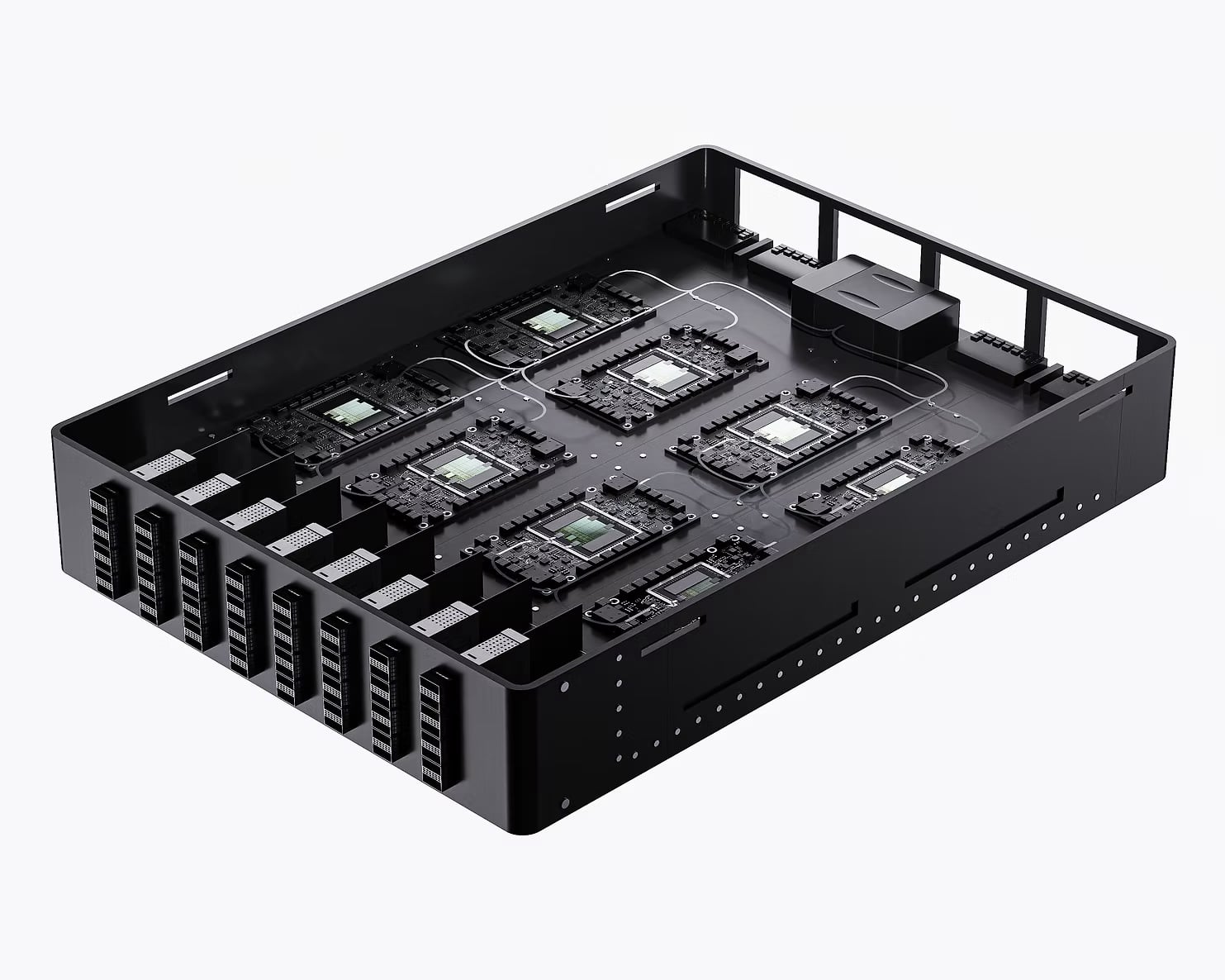
The figures Neurophos presents
In its public documentation, Neurophos showcases Tulkas configurations with two levels: the OPU module and the server system. Specifically, the company publishes specifications for T100 OPU and T100 Server, aimed at dense low-precision operations (FP4/INT4) with an additional layer for FP16/INT16.
Tulkas T100 OPU (module):
- 0.47 EXAOPS in dense FP4/INT4 MACs/GEMMs
- 235 TOPS/W (declared efficiency)
- 2 kW peak / 1 kW average power
- 768 GB HBM with 20 TB/s bandwidth
- 200 MB L2 cache
- Software support cited: Triton and JAX
Tulkas T100 System (server):
- 2 EXAOPS in dense FP4/INT4 MACs/GEMMs
- 10 kW peak / 5 kW average power
- 3.07 TB HBM with 80 TB/s
- 800 MB L2 cache
- Software cited: Triton and JAX
Some tech publications have amplified the impact of these figures with more aggressive interpretations — including references to a supposed “Tulkas T110” and internal speeds of tens of GHz — though such nomenclature is not prominent in the official corporate materials reviewed.
The key nuance: EXAOPS is not the same as “petaFLOPS”
Here, it’s important to distinguish marketing from engineering reality. When talking about EXAOPS (exa-operations per second) in FP4/INT4, it measures a very specific type of operation (usually MACs/GEMMs) at extremely low precision, relevant today for inference and certain quantization techniques. It’s not directly comparable to traditional FLOPS (FP32/FP64) nor to results from independent benchmarks. In other words: magnitudes are enormous, but the actual value depends on what workloads, what effective precision, what latencies, what memory, and what tools are available for a customer to use without rewriting their entire stack.
Neurophos also claims that its goal is a “drop-in” replacement in data centers, and that its technology could provide “up to 100×” improvements in performance and efficiency over current leading chips. This is a high-stakes assertion that, for now, remains at the level of corporate proclamation and must be validated through reproducible comparisons.
The geopolitical and industry angle: it’s not just “more performance”
Two additional layers explain why this announcement has gained traction:
- Capital dynamics and alliances: the funding round is led by Gates Frontier, with participation from M12 (Microsoft’s venture fund), along with firms linked to energy and sustainability. This signals that the “performance-per-watt” challenge is viewed as a strategic bottleneck, not just marginal optimization.
- The ecosystem is moving toward photonics: even when photonics is used primarily for interconnects (rather than computing), the goal remains the same: move more data with less energy and heat. This debate is closely tied to advanced packaging and system-level architecture.
The decisive question: lab prototype or platform?
For an OPU to become an infrastructure product, three tests are essential:
- Software and real adoption: promising Triton/JAX support is good headline material, but the market demands practical compatibility with workflows like PyTorch, TensorRT-like optimization, kernels, observability, and production tooling.
- Reliability and control: photonics and analog (“physical”) computing often require calibration, variation compensation, and noise management. Operational “day two” engineering is as important as raw performance.
- Integration with memory and networking: inference performance is rarely just about computation; data movement matters. HBM and TB/s figures are as critical as operation counts.
Neurophos states that it is accelerating toward hardware ready for developers and early deployments. If the project solidifies, it’s likely that the near future will resemble more a “mix” (GPU + specialized accelerators + photonics) rather than an instant replacement of a dominant player.
Frequently Asked Questions
What is an Optical Processing Unit (OPU), and how does it differ from a GPU?
An OPU aims to perform key operations (like matrix multiplications) using light within integrated photonic circuits, whereas a GPU executes them via electronic switching in transistors. The practical differences often relate to potential energy efficiency and how memory, signal conversion, and control are managed.
Why are FP4 and INT4 so important in AI inference?
Because many inference workloads tolerate low precision thanks to quantization techniques. Reducing precision boosts effective performance and reduces energy consumption, provided the model maintains quality and the system has sufficient memory and bandwidth.
Would an OPU be suitable for training models, or is it only designed for inference?
According to Neurophos, their primary focus is inference and dense MAC/GEMM operations at low precisions. Training involves different trade-offs (precision, numerical stability, communication, scaling), so it cannot be assumed to be directly supported.
What obstacles typically hinder photonic computing for AI?
Integration with software stacks, electro-optic conversion costs and latency, system calibration and noise control, operational reliability, and independent validation with real workloads.
Via: Neurophos whitepaper