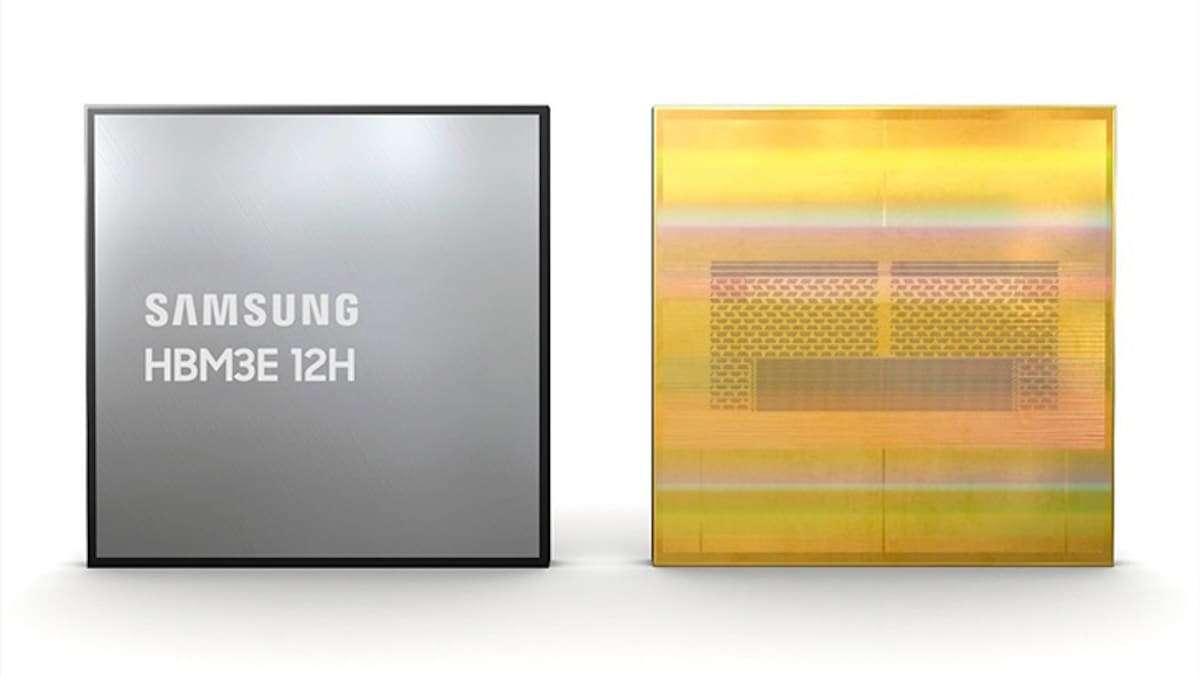
Samsung Electronics has taken a significant step forward in its high-bandwidth memory roadmap: the company has entered the backend design phase of its customized base die for the HBM4E (7th generation), a milestone often interpreted in silicon development as having surpassed the “halfway point” toward tape-out.
The focus is on a component increasingly crucial in the competition to supply memory for AI: the base die, the “logic substrate” at the bottom of the stacked HBM. In a market where customers no longer demand just capacity and bandwidth, but specific integrated logic functions within the memory, the base die has become a key terrain for product differentiation, stability, and integration with GPU/accelerator platforms.
Why the base die is now the battlefield
HBM is not just “stacked DRAM.” The base die acts as a control zone for the stack: it manages read/write operations to each DRAM die, implements ECC (Error Correction Code) mechanisms, and directly contributes to the stability and thermal behavior of the entire unit, especially when AI workloads push the memory subsystem to its limits.
The shift comes from major buyers: according to the provided material, customers are demanding custom HBM solutions with additional logical functions embedded in the base die. In other words, memory is moving away from being a “generic” component to becoming a co-designed element with customer-specific requirements (and potentially platform-specific ones).
What “entering backend” entails: closer to tape-out, higher execution demands
The backend phase is the physical design stage, where the chip transitions from a logical description (RTL or other front-end representations) to a real implementation: placement, routing, timing closure, signal integrity, power consumption, physical verification, and adaptation to the foundry flow.
Once the backend is complete, the design is delivered for tape-out (sent to the fabrication process). This transition is critical because, from this point onward, the margin for “cheap” modifications diminishes, and any major changes can impact scheduling and costs.
An internal roadmap shift and supply chain pressure
According to industry sources cited in the materials, Samsung has recently defined a new HBM roadmap, and has instructed its partners to prepare supply plans aligned with this new plan before March. The apparent goal: advance timelines compared to previous plans and strengthen its custom HBM strategy.
The roadmap includes:
- HBM4 (6th generation), with volume production planned for this year.
- HBM4E (7th generation).
- HBM5 (8th generation).
The industry expects to see HBM4E in 2027 and HBM5 in 2029, according to the provided information.
Table 1 — Cited Roadmap and Market Horizons (per the provided data)
| Generation | Name | Expected Focus | Mentioned Timeframe |
|---|---|---|---|
| 6th | HBM4 | More “general-purpose” | Volume production “this year” |
| 7th | HBM4E | Shift towards custom HBM | 2027 |
| 8th | HBM5 | More advanced custom HBM | 2029 |
Two teams: standard vs. custom, and increased staffing
A notable detail hinting at a major organizational change: according to a comment attributed to an executive from Shinhan Securities at a seminar, Samsung will operate two teams (standard HBM and custom HBM) starting from HBM4, and has allocated design personnel for custom HBM initiatives aimed at Google, Meta, and NVIDIA, with approximately 250 additional team members.
If this structure is confirmed, it clearly reflects market dynamics: future differentiation will not only be based on density or nominal speed but also on how the base die logic is integrated with the overall compute platform.
The critical point: co-design with the foundry and base die logic
The document emphasizes a key idea: while HBM4 predominantly features “more general” products, starting with HBM4E/HBM5, the industry is shifting toward custom memories, where how the base die logic is designed in collaboration with the foundry will be pivotal.
This collaboration is critical for three reasons:
- Physical compatibility and rules for the node and packaging.
- Signal integrity and latency in I/O interfaces (the “backbone” of effective performance).
- Verification and reliability: ECC, partial error management, and potential functions related to computing/thermal management.
The provided material indicates that Samsung is working on physical implementation and EDA environment optimization for the customized HBM4E base die. Also mentioned is the involvement of Lim Dae-hyun (memory interface expert, with previous experience at IBM and GlobalFoundries, who joined Samsung in 2023) in I/O design.
Technical schedule: most effort concentrated in backend
The development of an HBM design typically takes around 10 months, according to the text. Within this cycle, the backend would account for approximately 60–70% of the work, with an approximate breakdown of 4:6 between front-end and back-end. It is also stressed that during the backend, revisions and cross-verifications with front-end occur.
Following this logic, the design of the custom HBM4E could be completed by May or June (per the provided info), though mass production and qualification milestones depend on additional factors.
Table 2 — Workload distribution in design (per cited ratios)
| Stage | Scope | Estimated share in the cycle |
|---|---|---|
| Front-end | Logical design (RTL), architecture, functional verification | ~40% |
| Back-end | Physical design, placement & routing, closure, physical verification, delivery to tape-out | ~60–70% |
Competitors: SK hynix and Micron in similar phases
Another relevant point: the text suggests that Samsung, SK hynix, and Micron are advancing in comparable phases of customized HBM4E development, and that no company is clearly ahead or behind at this stage. In a market driven by supply cycles and demanding validation processes, the “phase snapshot” can be just as important as raw performance.
JEDEC and HBM5: standards in parallel with product development
Finally, it is indicated that Samsung’s memory division is involved in standardizing HBM5 within JEDEC, while also progressing with product planning. This simultaneity — standards and development running in parallel — is common in memory, but becomes particularly relevant when the market pushes towards customer-specific requirements.
Indeed, the materials suggest that from HBM4 onward, customers are requesting to embed functions such as computing capabilities, thermal control, or partial error management in the base die. Meanwhile, competitors are also preparing separate lines for both general-purpose and custom solutions.