High-NA EUV lithography has been embedded in the industry’s imagination for years as the key lever to continue shrinking geometries when traditional scaling begins to confront physical limits. However, among technical circles and expert calls, a less epic and more grounded message is gaining traction: buying a machine does not equal the ability to manufacture at volume. The prevailing thesis, repeatedly emphasized in recent industry discussions, is that the true indicator of High-NA maturity is not just the hardware from ASML, but the maturity of the “ecosystem” surrounding it. Within that ecosystem, there is always a component that arrives before everything else: OPC (Optical Proximity Correction).
The debate resurges around a specific question: Is Intel encountering obstacles with High-NA EUV for its 14A node due to OPC and process flow readiness issues? This is a significant question because Intel has positioned High-NA as a differentiating factor in its roadmap to regain momentum in advanced node development. Meanwhile, from Taiwan comes the other side of the debate: TSMC continues evaluating High-NA but does not appear ready to adopt it in the short term, even in logic generations where, on paper, it could provide advantages in mask complexity.
Why High-NA isn’t “plug and play”
High-NA EUV (0.55 NA) promises greater resolution than conventional EUV (Low-NA), enabling reductions in multi-patterning and simplifying certain steps. That’s the theory. Practically, the industry argues that introducing such a tool demands much more than recalibrating the scanner: materials, masks, metrology, process control, variability, overlay, and especially, computing.
In this chain, OPC stands as the “first gate.” Optical Proximity Correction, in simple terms, involves techniques that adjust the mask pattern so that the printed wafer feature matches the intended design, compensating for optical and process distortions. As nodes become more aggressive, OPC becomes more demanding. And as optical regimes shift — as happens when moving to High-NA — more work is needed to adjust models, calibrations, and verification flows.
That’s why a warning heard from experts in recent calls is circulating: even if Intel possesses High-NA tools, OPC “may not be ready” to support a direct move to volume production, because the entire ecosystem is still under development. The same conversation highlights a critical temporal factor: an advanced node is “frozen” years ahead in many aspects. If the flow isn’t ready in time, it becomes very challenging to introduce it without jeopardizing schedules.
TSMC, the other side: pragmatism and schedule
Similarly, TSMC’s stance in technical discussions is cautious. The company has publicly stated that it continues evaluating when to adopt High-NA, but does not yet see a clear need for certain generations, especially considering cost and return. Their assessment isn’t purely technological: it includes actual throughput, stability, cost per wafer, and comparisons with alternatives based on Low-NA with multi-patterning and process optimization.
By May 2025, Reuters reported that TSMC was still evaluating High-NA and citing concerns over price and the lack of a sufficiently compelling incentive for certain stages of their roadmap. Looking ahead to 2026, the expectation is that if TSMC perceives no clear cost/risk advantage, it will delay adoption, even if Intel tries to use High-NA as a differentiator.
At the same time, TSMC has also announced that it does not plan to use High-NA in its A14 node, reinforcing a cautious strategy: squeezing the most out of Low-NA, managing mask counts, and avoiding premature cost increases.
Intel 14A: visible investment, invisible doubts
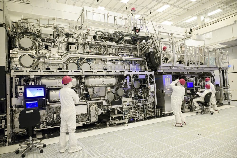
For Intel, deploying High-NA has become a symbol of industrial ambition. Recently, it was reported that a High-NA production tool (EXE:5200B) was installed as part of the path toward 14A, marking a significant milestone since it moves beyond R&D and closer to actual manufacturing, where yields, reliability, and repeatability are key.
However, even with the machine in place, success depends on the overall alignment: if OPC, validation, and control flows are not at the volume-ready level, High-NA risks remaining a partial advantage (limited layers, phased deployment) or a future bet rather than an immediate leadership driver. Furthermore, in 2025, signals indicated that Intel was already considering alternative paths to avoid being restricted by High-NA availability and maturity — a way to “cover themselves” against schedule risks.
This approach aligns with what was heard in expert calls: Intel might have “some margin” behind TSMC at certain points, but not enough to wait indefinitely for the High-NA ecosystem — especially OPC — to reach industrial readiness.
What’s truly at stake: credibility, costs, and customers
Beyond technical debates, a business dimension is equally critical. High-NA involves extremely costly tools and a capital commitment that only makes sense if the node attracts enough volume, particularly in foundry services for third parties. In this context, questions about the ecosystem’s readiness (including OPC) aren’t mere technicalities; they’re signals of potential risk for customers who base their designs years in advance.
The paradox is that High-NA was promoted for years as “the ultimate solution” to avoid multi-patterning complexities, but now the conversation shifts to less glamorous aspects: software, models, calibration, and computational capacity for OPC. In other words, the bottleneck might not be the machine itself but the set of invisible components needed to turn it into reliable production.
In the short term, the industry appears to be balancing two strategies: Intel working to position High-NA as a key differentiator with 14A, and TSMC adopting a pragmatic stance, delaying its use until the cost/risk equation improves or a specific generation demands it. Between them, a recurring lesson emerges: in semiconductors, innovation isn’t just “installed”; it’s industrialized.
Frequently Asked Questions (FAQ)
What is OPC in lithography and why could it slow down High-NA EUV adoption?
OPC (Optical Proximity Correction) adjusts mask patterns so that the printed wafer features match the design despite optical and process distortions. In High-NA, optical conditions and tolerances change, requiring more complex models and calibrations; if this flow isn’t mature, volume manufacturing becomes more complicated.
Why might TSMC delay using High-NA EUV in A14 and even hesitate on A10?
The decision is driven by schedule and wafer cost: if Low-NA EUV with optimization and multi-patterning techniques suffice, TSMC can postpone High-NA until it becomes necessary or clearly economical.
What does it mean that Intel installed an EXE:5200B High-NA EUV tool?
It’s a significant industrial milestone: the tool is designed for production environments, not just R&D. However, installing it doesn’t ensure immediate high-volume use; integration of the entire ecosystem (materials, metrology, OPC, control) is essential.
Does High-NA EUV always reduce mask counts and lower chip manufacturing costs?
Not necessarily. It can simplify certain layers, but tool costs, process complexity, and ecosystem maturity may offset or even outweigh those benefits in early phases.