For years, talking about Tesla and its proprietary semiconductors was primarily about Dojo: an internal supercomputer designed to train models using data from its assisted driving and robotics ambitions. But in recent months, the focus has shifted to another piece: Tesla’s AI chip family (AI5, AI6, and beyond), which the company aims to turn into a common platform for cars, robots, and data centers. In this transition, Elon Musk’s giant is moving pieces on two fronts: speeding up design cycles and restructuring the supply chain.
The most striking catalyst came with a direct statement from Musk himself: “solving AI5 was existential” for the company. This phrase is significant: it suggests that without that silicon leap, the rest of the artificial intelligence strategy—from autonomy to large-scale training—would be left hanging. Since then, Musk has defended a roadmap targeting a design cycle of about nine months for upcoming generations (AI6, AI7, AI8, AI9), a pace intended to narrow the gap with the typical yearly cadence of major accelerated computing players.
From “everything with TSMC” to a layered model
Beyond scheduling, the other major story revolves around how that silicon is manufactured and packaged. In its early iterations, Dojo was associated with a very specific strategy: large modules built from 25 D1 chips, integrated into a “training tile,” an approach linked to advanced System-on-Wafer packaging techniques that interconnect multiple dies into a large assembly. Such integration offers clear advantages for training: extreme internal bandwidth and an architecture designed for scalable, compact blocks. But it also comes with costs: industrial complexity, dependence on very specialized capabilities, and a manufacturing process that’s not always compatible with volumes typical of the automotive industry, where millions of units are produced.
Within this context, industry reports have circulated suggesting a break from the traditional “single partner handles everything” approach. The thesis is that Tesla is exploring a bifurcated model for Dojo 3, with Samsung Foundry handling front-end manufacturing and Intel managing advanced packaging (back-end) to build modules. If confirmed, this move would be significant for two reasons: technically, because of the ambition to produce large, interconnected modules; strategically, because of the diversification and capacity-negotiation in a market with advanced nodes and tight packaging constraints.
Samsung, Intel, and the packaging battle: EMIB as a key piece
Packaging increasingly defines a chip’s competitiveness. Here emerges EMIB—Intel’s 2.5D technology based on embedded silicon bridges in the substrate that connect multiple dies without needing a full-sized interposer. In theory, this approach allows more flexibility with chiplet integration, reduces certain geometric constraints, and enables the design of scalable modules built from interconnected blocks.
For Tesla, the appeal of a modular packaging approach is obvious: if the goal is for one silicon to serve cars (few chips), robotics (similar configurations), and servers (many chips), then the architecture needs to grow in an industrializable way. While this doesn’t eliminate challenges—such as yields, heat dissipation, interconnection, and reliability—it shifts the focus from “exotic” full wafer fabrication to reusable modules.
AI6 and a multi-billion-dollar contract: capacity and industrial sovereignty in the U.S.
Ahead of Dojo, Tesla signaled clarity with AI6. Samsung announced a major manufacturing agreement, and Musk publicly linked it to Tesla, indicating that a Samsung factory in Texas (Taylor) would produce the AI6 chip. Public documents and economic reports mention a contract volume of 22.76 trillion won (roughly $16.5 billion), highlighting the scale: this isn’t just an experiment but an effort to reserve capacity for a platform Tesla plans to deploy across multiple product lines.
The implicit message is twofold: first, to secure supplies amid global bottlenecks for advanced nodes and frontier packaging; second, to establish manufacturing capacity in the U.S., aligning with broader trends to attract advanced production through incentives and anchor clients.
And TSMC? A nuanced transition, not a clean break
Although some headlines have interpreted these developments as a total break, the broader picture from various sources suggests a more nuanced approach. Musk has previously highlighted a dual-sourcing strategy for certain generations, involving both Samsung and TSMC depending on the chip and schedule. The industry has been reading AI5/AI6 as a phase where Tesla seeks to maximize options: balancing performance, cost, capacity, and risk.
This nuance is key to understanding Tesla’s business logic: relying on a single manufacturer is efficient when everything goes smoothly, but it’s a risk in increasingly short development cycles. With an accelerated iteration plan, any delay—whether in yields, ramp-up, packaging, or validation—could jeopardize a launch.
Dojo 3 back on the table: from “on hold” project to internal platform component
The Dojo story has also evolved. In 2025, reports indicated Tesla was reorganizing its Dojo efforts, focusing on next-generation chips and relying more on external suppliers for training. However, early 2026 brought a different message: with AI5 “on track,” Musk hinted that Tesla resumes development of Dojo 3. In other words, Dojo is not disappearing but changing role—shifting from a standalone project to an ecosystem component where proprietary silicon (AI5/AI6 and successors) can scale from edge devices to data centers.
The ultimate ambition appears to be an extreme vertical integration: Tesla designing the chip, defining its packaging, and orchestrating deployment across cars, robots, and clusters. This approach is costly, complex, and technically risky, but it aligns with Musk’s vision of gaining independence from the roadmaps of NVIDIA, AMD, or third parties—especially as the business pivots towards practical AI applications.
Frequently Asked Questions
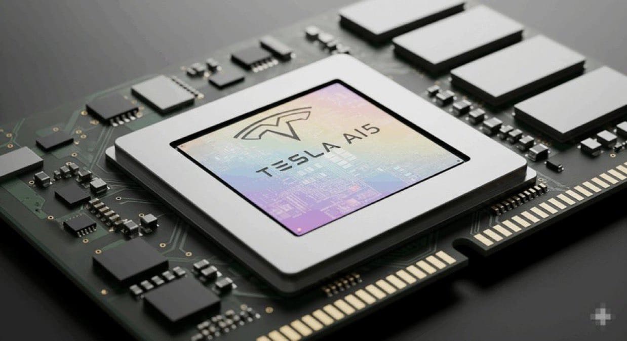
What are Tesla’s AI5 and AI6 chips, and what will they be used for?
They are Tesla’s processors designed to accelerate AI tasks within its products. The company links them to assisted driving systems, humanoid robotics, and at a broader level, to training infrastructure and server computing.
Why is advanced packaging (like System-on-Wafer or EMIB) so critical in Dojo?
Because it determines how multiple chips connect to form a larger system. In model training, interconnection quality and bandwidth directly impact performance and energy efficiency.
Is Tesla abandoning TSMC for Samsung and Intel?
The available information points more toward diversification rather than a complete abandonment: Tesla aims to combine partners based on generation, capacity, and manufacturing/packaging needs, reducing dependence on a single supplier.
Is a 9-month chip design cycle realistic?
This is an aggressive industry target. Tesla sees it as an acceleration goal, but feasibility depends on factors like node complexity, verification, yields, EDA tools, and packaging/test availability at scale.
Source: Jukan X