The race to “relocalize” the Artificial Intelligence (AI) value chain in the United States reaches a new milestone marked on the calendar. Micron Technology has announced that January 16, 2026 will mark the official start of construction on its large-scale advanced memory factory in Onondaga County (in the Clay area, in the central part of New York State), a project valued at $100 billion that the company describes as the largest semiconductor manufacturing facility in the country’s history.
This announcement is not just a ceremonial gesture. According to Micron, it follows the completion of environmental reviews and permits necessary to begin land preparation and construction. The day will bring together company executives with federal, state, and local officials, culminating in a series of events at Syracuse University. In the words of CEO Sanjay Mehrotra, it is a “decisive moment” for the company and for the United States, as the economy makes a sweeping move into the AI era.
Memory is “not just a component”: it’s the bottleneck of AI
The key is that memory — DRAM, NAND, and increasingly HBM (High-Bandwidth Memory) — has become one of the factors that influences the pace of AI deployment at scale. Models are growing, data centers are multiplying, and with them, the need to move and supply data rapidly. Without enough advanced memory, the rest of the system (GPUs, networks, CPUs, and software) loses efficiency.
This logic underpins Micron’s investment: a facility with up to four fabs aiming to establish cutting-edge memory production capacity on U.S. soil, especially as the global supply of critical components has become a matter of economic and national security.
Moreover, the project is closely linked to U.S. industrial policy. The official CHIPS program webpage (NIST/Department of Commerce) details that Micron received $6.44 billion in direct funding to support its two-decade vision: investing roughly $100 billion in New York and $50 billion in Idaho, with the goal of increasing American-made advanced memory from less than 2% now to around 10% by 2035. The same framework also mentions funding for workforce development and restrictions tied to CHIPS Act incentives, a reminder that reindustrialization comes with conditions.
Employment estimates vary depending on scope (direct, indirect, and supply chain). The project has been declared the largest private investment in New York State’s history and, according to Reuters, is associated with the creation of more than 50,000 jobs over 20 years, including both direct and induced employment. The energy infrastructure is also being prepared: the state approved a 345 kV underground transmission line to connect a nearby substation with the future site, a practical reminder that the chip industry is also an electrical industry.
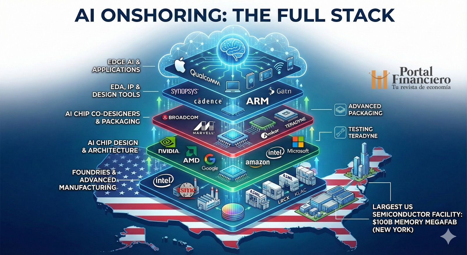
“Onshoring” of AI: the full map extends far beyond memory
Micron’s announcement reflects a growing sector insight: memory is just one layer. Relocating AI involves tightening (and rebuilding) an entire industrial “stack,” from design to final packaging.
1) AI chip design (and the tug-of-war between hyperscalers and suppliers)
Training and increasingly inference revolve around GPU platforms, where NVIDIA maintains a dominant position in training, according to Reuters market analysis. But the landscape has become more competitive: AMD is strengthening its role as a strategic alternative; Google is pushing TPUs optimized for training and inference; and AWS is developing Trainium and Inferentia to reduce cloud costs. Meanwhile, Microsoft promotes a “silicon-as-a-service” approach with its own chips for Azure, aiming to optimize its infrastructure end-to-end.
2) Co-design: custom systems built “to order”
Meanwhile, the rise of custom silicon is pushing players like Broadcom and Marvell — often mentioned as technology partners — to co-design components and systems that integrate compute, memory, and networking architectures tailored for specific AI workloads.
3) EDA and IP: the invisible toll before fabrication
Before a chip exists, it must be designed and validated using EDA (Electronic Design Automation) tools. Synopsys and Cadence are repeatedly identified as foundational players: without their platforms, moving from design to a “functional silicon” becomes more difficult. Additionally, CPU intellectual property (IP), notably Arm with its widely licensed architectures, supports a significant portion of mobile, edge, and increasingly server computing.
4) Foundries: who fabricates the design (and where)
Although the U.S. promotes a return to domestic manufacturing capacity, the industry still relies heavily on large foundries: TSMC remains a central pillar of the global advanced chip supply. Meanwhile, Intel aims to position itself as a “second source” with its foundry and domestic manufacturing efforts — a strategic move in a geopolitically influenced world where capacity and timelines are affected by international tensions.
5) Equipment: the true “center of gravity”
In modern manufacturing, few names are as critical as ASML, whose lithography equipment (including the EUV family) is essential for leading-node logic and advanced DRAM production. Around it, Lam Research, KLA, and Tokyo Electron—among others—provide deposition, etching, metrology, and process control tools that enable large-scale production. Applied Materials and Teradyne complete critical stages such as material processes, implantation, testing, and validation.
6) Advanced Packaging: turning memory and compute into systems
Lastly, the often-deciding layer for actual performance: packaging. Integrating GPUs with HBM and other components into advanced modules requires specialized industry expertise. Companies like Amkor are key players in this stage, helping to “convert chips” into ready-for-data-center compute systems.
7) Edge AI: relocalizing AI into pockets
Relocalization isn’t just about massive factories. Apple, with its Neural Engine and focus on on-device machine learning, exemplifies the trend of bringing inference directly to the end user, offering privacy and latency benefits. Qualcomm works on NPUs and tools to accelerate inference on mobile devices and endpoints, bolstering the role of edge in the overall AI architecture.
Subtle message: AI is already an industrial policy issue
Micron’s mega-project, beyond its scale, signals that AI is no longer just a software race. Today, it’s also a race involving factories, energy, talent, and supply chains. In this race, the U.S. is trying to rebuild pieces that have been concentrated outside its borders for decades.
The open question is whether the full industrial “stack” will synchronize successfully. Building advanced memory is a huge step, but onshore AI will only become truly tangible when design, tools, fabrication, equipment, packaging, and deployment fit together with the same precision demanded by the chip itself.
Frequently Asked Questions
Why is HBM memory so important for generative AI in data centers?
Because it supplies accelerators (like GPUs) with bandwidth far exceeding traditional memories, avoiding bottlenecks during large-scale training and inference.
What does it mean that Micron is “the only U.S. manufacturer of memory”?
It signifies that, amidst a historically Asia-centric market for advanced memory, Micron represents the U.S.’s domestic industrial backbone for this segment, which is critical for supply resilience and security.
How does the CHIPS Act influence projects like Micron’s large factory in New York?
It provides incentives and public funding to accelerate private investments, with conditions and milestone tracking aiming to increase the domestic production capacity of strategic semiconductors.
Which parts of the AI industrial “stack” are hardest to relocate?
Those heavily dependent on highly specialized machinery and know-how (lithography and manufacturing processes), and those requiring mature ecosystems (EDA, advanced packaging, supply chain, and skilled workforce).
Source: Portal Financiero