The race for artificial intelligence isn’t just fought on GPUs or the next generation of lithography. Increasingly, the battle is decided in a less visible phase for the general public but critical to delivering chips on time and with quality: advanced packaging. This is where SK hynix — one of the main drivers of the HBM memory boom in data centers — has decided to accelerate strongly.
The South Korean company confirmed the construction of a new packaging and testing plant in Cheongju (North Chungcheong Province), called P&T7, with an investment of 19 trillion won (approximately $12.92 billion). The project will be built on a 230,000 square meter site within an industrial complex of the city. According to official sources and local press, construction is scheduled to begin in April 2026 and be completed by late 2027.
Beyond the magnitude of the figures, what’s most significant is what they represent: memory alone is no longer enough. In the AI supply chain, manufacturing chips is just one part of the problem. The other, increasingly limiting factor, is assembling and validating those high-value components — stacked memory, interposers, high-density connections, thermal management — to turn them into ready-to-integrate products for accelerators and servers.
From manufacturing HBM to “delivering the complete system”
In SK hynix’s terminology, P&T means “packaging and testing”: the set of back-end processes that transform finished chips on wafers into end products, with final inspection and quality verification. This is a key point to understand why the company is moving so assertively.
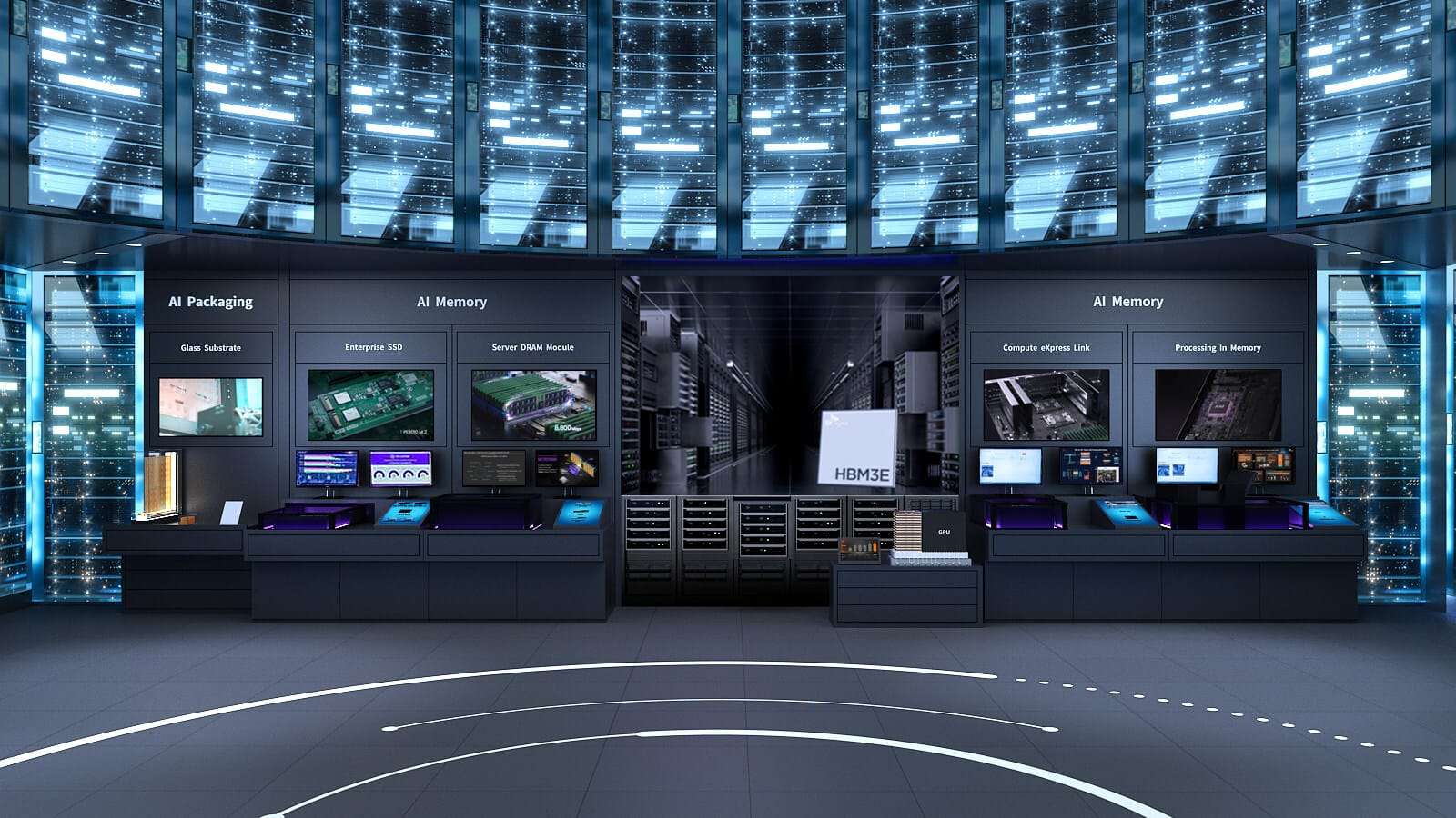
In the AI ecosystem, HBM (High Bandwidth Memory) has become a strategic component. Not only because of its performance but because its availability dictates the deployment pace of training and inference clusters. However, HBM isn’t a “traditional” module: it requires complex stacking techniques and, above all, advanced packaging to efficiently integrate it with compute chips.
SK hynix aims for Cheongju to function like a kind of “campus” where production and packaging are organically connected. The company envisions P&T7 as a gear designed to operate in tandem with its local facilities, including M15 and especially M15X, a plant focused on advanced memory. According to announcements, this connection would strengthen Cheongju as a central hub for AI memory, reducing logistical frictions and increasing responsiveness to demand surges.
The bottleneck reshaping the industrial map
For years, discussions about dependency on semiconductors focused on “foundries.” But the AI boom has shifted some of the risk to another segment: advanced packaging capacity.
Modern AI platforms require integrating compute, memory, and connectivity at a density that demands techniques like 2.5D/3D packaging and highly precise assembly processes. If this “back-end” becomes saturated, the unthinkable happens: you can have ready chips… but you can’t convert them into final products at market speed.
Therefore, SK hynix’s move can also be seen as an industrial power play: who controls packaging controls timelines, margins, and access. It’s not just about manufacturing more but about reducing dependency on third parties and offering a more comprehensive solution to clients investing billions in AI infrastructure.
A strategy also looking toward the United States
The focus on packaging isn’t limited to South Korea. Meanwhile, SK hynix has been preparing for expansion into the U.S., centered around an advanced packaging and R&D center linked to incentives from the CHIPS Act, with public funding announced by the U.S. Department of Commerce.
This kind of deployment shares a similar goal: approaching demand, safeguarding the supply chain, and positioning as an “end-to-end” provider in a market where each quarter counts. The logic is clear: if packaging becomes a global bottleneck, having capacity that’s both in-house and geographically distributed ceases to be an advantage… and becomes a necessity.
The geopolitical backdrop: industry, territory, and resilience
In South Korea, the decision to locate P&T7 in Cheongju has been framed as part of a strategic move aligned with regional balance policies and long-term industrial strengthening. In other words, it’s not merely a corporate investment but a piece within the debate on how to distribute strategic industry and where to create high-skilled jobs.
The message to the market is powerful: AI memory cannot depend on a fragmented supply chain if scalability from “niche” to “mass infrastructure” is to be achieved. In this new world, SK hynix aims to move beyond being simply a key component manufacturer and become increasingly a player that also controls the final step: transforming that memory into deployable computing capacity.
Frequently Asked Questions
What is advanced packaging, and why is it crucial for AI HBM memory?
Advanced packaging encompasses techniques that enable high-density, efficient integration of compute chips and memory. For AI, HBM requires this type of packaging to achieve its bandwidth and performance, and industry capacity directly influences server deployment rates.
What exactly will SK hynix’s new P&T7 plant in Cheongju do?
P&T7 will focus on “packaging and testing”: transforming finished chips into final products with validation and quality control, reinforcing the final stage of production for memory solutions destined for AI.
Why is packaging seen as a bottleneck in the AI supply chain?
Because the demand for accelerators and advanced memory is outpacing the capacity to assemble and validate these components using 2.5D/3D techniques. If packaging can’t scale, the final product will be delayed even if chips are available.
How might this investment impact HBM availability for data centers?
Expanding in-house packaging and testing capacity should help reduce bottlenecks and lead times, improving the supply rhythm of critical AI components, especially during demand surges.
via: wccftech