South Korea’s largest industrial project to strengthen its chip manufacturing —and, incidentally, secure its role in the Artificial Intelligence economy— has just crossed a critical line from plan to reality. Samsung Electronics and the public corporation Korea Land and Housing Corporation (LH) have finalized the land sale agreement linked to the Yongin Advanced System Semiconductor National Industrial Complex. This move unlocks the project’s direct entry into the execution phase and accelerates a timeline the government has been pushing for months.
According to reports from Korea, LH signed the purchase contract with Samsung and nearly immediately moved to the next step: negotiating compensation with landowners and asset holders (buildings, structures, trees) within the designated project perimeter. Just five days after these negotiations began, progress stood at 14.4%. While an early figure, it’s significant because it indicates the project is no longer just an announcement — it’s an operational, administrative, and social process underway.
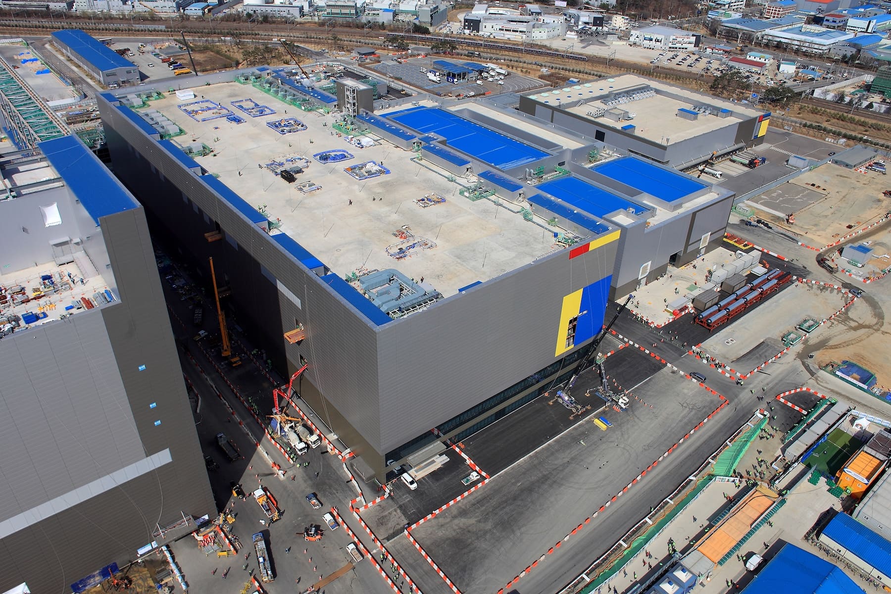
A “Mega-Cluster” with Six Factories and Ambitions to Become a Global AI Chip Hub
The Yongin complex (Gyeonggi Province) is conceived as a core part of South Korea’s “mega-cluster” semiconductor initiative. The immediate plan covers an area of 7,773,656 m² (approximately 2.35 million ping, according to local press), where Samsung will develop six logic/system semiconductor manufacturing facilities along with supporting buildings. Surrounding this core, an industrial ecosystem is envisioned: plans include the entry of dozens of material, component, equipment, and design companies, together with research centers.
Investment figures in Korea are enormous: Samsung has announced plans totaling around 360 trillion won for this enclave (with expectations that the total could grow as construction progresses and new phases begin). On a broader scale, the Korean government describes its “Semiconductor Mega Cluster” strategy as a 622 trillion won project—incorporating industrial hubs and related supply chains—a scale designed not only to boost capacity but to enhance resilience and speed.
The core message is clear: in the AI race, talent and design are not enough; manufacturing and packaging capacity close to a responsive industrial fabric are essential. This translates into factories, supply chains, and logistics operating in a “war-time” mode of technological urgency.
Timeline: Construction Bidding and Start-up in 2026, with aiming for First Operations by 2030
The roadmap follows two main tracks: the land acquisition (compensation and availability) and the permits/planning (approvals and impact assessments). South Korea has long sought to shorten the usual timelines of such developments through expedited procedures and inter-agency coordination involving ministries, local governments, Samsung, and LH. By 2024, a public “cooperation” agreement indicated a target to start construction in 2026 and to operate the first factory before the end of 2030—aiming to keep pace with soaring demand cycles.
Recent updates suggest LH plans to issue construction tenders and launch large-scale work in the second half of 2026, once land availability is secured.
This phase—covering land acquisition plus civil works—is critical: it separates “strategic planning” from “actual capacity”. In semiconductors, delays are costly; a late factory might find its market already shifted or customers switching to other regions.
The Bottleneck: Energy, Water, and the Politics of Location
Progressing such a large project doesn’t mean it’s free of friction. In Korea, the conversation around energy and resources has become prominent: media reports have cited statements attributed to a minister regarding the electrical impact of concentrating factories in Yongin, with comparisons to several nuclear power plants. The controversy prompted clarifications, emphasizing that the remarks reflected challenges in grid infrastructure and the importance of “producing close to where energy is consumed”.
This is no minor detail. In the semiconductor sector, bottlenecks go beyond lithography: stable electricity, ultrapure water, grid infrastructure, and talent are equally vital. Yongin’s location is strategic because of its proximity to existing Samsung industrial hubs, suppliers, and technical service centers—factors that in high-complexity factories translate into hours or days of operational availability.
Global Significance: Industrial Sovereignty and Supply Chain Resilience
From a broader perspective, Yongin isn’t just a local project. It aligns with international trends seen in the US, Europe, Japan, and India: reindustrializing parts of the supply chain, reducing dependence on external sources, and ensuring supply can meet the exploding demand for AI-related chips.
Moreover, this timing is particularly sensitive given the cyclical nature of foundry markets: when a leading node becomes saturated, the industry—including clients and governments—react sharply. Each megaproject becomes a message: “We will have capacity, scale, and continuity”.
In essence, Yongin embodies South Korea’s strategic bet to preserve what it considers vital: advanced chips, production capacity, and geopolitical leverage.
Frequently Asked Questions
What exactly is the Yongin semiconductor complex, and why is it called a “mega-cluster”?
It’s a large industrial zone focused on advanced semiconductors, designed to cluster factories, suppliers, and R&D centers in one area with public-private coordination to streamline permits and infrastructure development.
When will construction start, and when is the first factory expected to be operational?
Official plans target beginning construction in 2026, with the goal for the first factory to be up and running before the end of 2030. The schedule depends on progress in compensation and approvals.
What chips will Samsung produce at Yongin: memory or logic?
The plans presented in Korea describe Yongin as a hub for system semiconductors (logic/system chips), with six manufacturing facilities planned—this isn’t just a memory expansion.
What is the biggest risk for the project: technology, funding, or infrastructure?
In projects of this magnitude, the most immediate concerns often revolve around infrastructure (electricity, water, network connectivity) and land management (compensation and permits), rather than the technology itself, which proceeds in parallel.