The race to continue shrinking transistors—and, consequently, boost performance and efficiency in chips for data centers, high-performance computing, and AI workloads—is playing out on two fronts: more precise lithography and new architectures/materials that enable continued scaling as silicon approaches its physical limits.
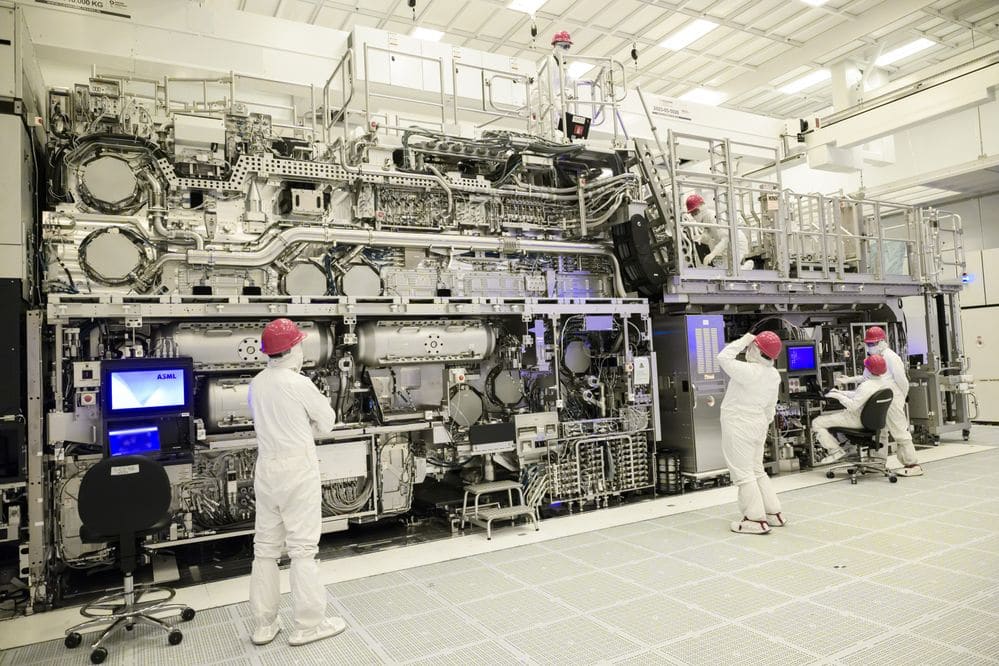
This dual effort is reflected in the latest milestone shared by Intel Foundry, which announced progress in two distinct projects connected by a common goal: turning lab innovation into manufacturable processes. On one hand, the company has achieved, alongside ASML, acceptance testing of the TWINSCAN EXE:5200B, one of the most advanced High NA EUV lithography systems. On the other, Intel and Imec presented results on integrating 300 mm wafers with 2D materials transistors, a research direction aimed at extending miniaturization beyond what silicon can support in the future.
High NA EUV: From “It Works” to “It Produces”
In lithography, demonstrating that a new tool can print finer patterns isn’t enough. The real challenge is turning that capability into productivity, repeatability, and control at rates compatible with modern manufacturing. Intel’s announcement places the EXE:5200B precisely at this point: moving from technical validation to production-relevant metrics.
According to shared data, the EXE:5200B maintains the high resolution of the first-generation system (EXE:5000) but raises the bar in two particularly sensitive indicators:
- Up to 175 wafers per hour output, a figure indicating productivity suitable for advanced manufacturing environments.
- Overlay of 0.7 nanometers, meaning improved precise alignment between lithographic layers—crucial when every nanometer matters and any mismatch leads to performance or yield losses.
The collaboration with ASML is also built on prior experience: Intel recalls that its work with High NA EUV began in 2023 with the arrival of the first commercial High NA tool at its R&D fab in Oregon. Since then, the focus has been on validating not just resolution but also the “ecosystem” making high-NA lithography viable at scale: masks, etching, metrology, and resolution enhancement techniques.
What Changes with the EXE:5200B
On a technical level, Intel describes three enabling innovations that explain why this generation matters:
- Higher power EUV source
More power means faster exposure at practical doses, a better process window for high-contrast patterns, and a key goal: reducing imperfections like line edge roughness and line width variation, problems that become more visible as patterns shrink. - New wafer stocker architecture
At first glance, it sounds logistical, but in advanced manufacturing, logistics is physical: thermal stability, consistent lot handling, and less operational drift. This is especially vital for flows requiring multiple passes or exposures, where any variation is amplified. - Stricter alignment control
The 0.7 nm overlay is attributed to advances in stage control, sensor calibration, and environmental isolation. Translated: greater control over system behavior under real conditions, essential for integrating High NA EUV in critical layers.
The benefit presented to designers isn’t just “more science,” but more flexible design rules, potential to reduce steps and masks, resulting in a simpler process that should, in theory, lead to better yields and a faster ramp to stable production. Intel emphasizes, however, that the industry is still in early phases of adoption.
Beyond Silicon: 2D Transistors on 300 mm Wafers
The second front is more long-term but equally strategic. Intel proposes an increasingly common idea in research forums: at some point, features will be so tiny that silicon atoms no longer behave “ideally” for performance enhancement.
Here come 2D materials, capable of forming layers just a few atoms thick. Intel cites the family of transition metal dichalcogenides (TMDs) as promising candidates for their current control and scalability. The open challenge is transitioning from lab advances to manufacturing in 300 mm wafers.
Against this backdrop, Intel and Imec presented at IEDM a key advance: a manufacturable integration on 300 mm wafers of source/drain contacts and gate stack modules for 2D transistors (2DFETs), using:
- WS₂ and MoS₂ for n-type
- WSe₂ for p-type
The core of this approach is a selective oxide etch applied to high-quality 2D layers grown by Intel, which were capped with an AlOx/HfO₂/SiO₂ stack. This enabled the creation of damascene-style top contacts, embedding metal within trench-like structures, without damaging the underlying 2D channel.
The underlying message is clear: one of the main bottlenecks for 2DFETs isn’t just “whether the material works,” but whether it can be realistically manufactured with contact and gate modules compatible with production-level integration.
“Manufacturability” as a Key Word
Intel summarizes both milestones with a core thesis: useful innovation is the one integrated with discipline. It transforms novelty into reliability and reduces surprises when moving from research papers to tape-in. In this context, “open” collaboration with companies like ASML and Imec accelerates learning curves, shares process insights, metrology, and failure modes, allowing clients and the ecosystem to operate under more realistic design constraints.
The takeaway for the industry is that the path toward next-generation chips—especially for AI workloads and high-performance systems—relies not on a single breakthrough but on a combination: more capable tools (High NA EUV) and new materials/architectures (2D). Both must demonstrate something critical that’s often more challenging than headlines: manufacturability at scale.
FAQs
What is High NA EUV and why does it matter for next-generation chips?
It’s an evolution of EUV lithography that aims to print finer, more precise patterns. In advanced nodes, this can simplify processes (fewer steps and masks) and improve performance and yield.
What does “overlay of 0.7 nm” mean in lithography tools?
It measures the alignment accuracy between layers. The smaller, the more precise the overlay, which is crucial for avoiding defects and performance loss in advanced tech.
Why are 2D materials considered future alternatives to silicon?
Because at very small scales, silicon’s ability to improve performance diminishes. 2D materials promise ultra-thin channels with good current control, but their manufacturability on 300 mm wafers remains an open challenge.
What does damascene integration bring to 2D transistors?
It allows forming top contacts via a compatible process, embedding metal in trench-like structures without damaging the 2D channel—key for scalable device fabrication.
via: community.intel