The so-called “technological decoupling” between China and the West has just taken a new step. The analysis of the new Kirin 9030 SoC confirms it is manufactured by SMIC using their N+3 node, an evolution of their previous N+2 (7 nm class) process, which in practice brings Chinese foundries closer to the 5 nm scale… but without using EUV lithography, the key equipment component that US bans have blocked.
It’s not yet a “5 nm” at the level of TSMC or Samsung, but it’s a clear signal that China continues progressing along its own technological path, even if only by pushing DUV tools to their limits and making manufacturing more complex.
What is N+3 and what does it mean for the Kirin 9030
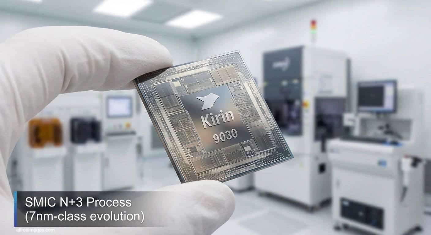
The Kirin 9030 is a next-generation application processor, and all signs point to it being the core of Huawei’s future high-end phones. Independent analyses agree that it is fabricated with SMIC’s N+3 process, described as a scaled extension of the N+2 7 nm node.
Simply put:
- N+2 would be “SMIC’s 7 nm,” already seen in chips like the Kirin 9000S.
- N+3 takes that same process one step further, reducing critical dimensions (especially the metal pitch) and applying design optimizations (DTCO, design–technology co-optimization).
In terms of transistor density and physical scaling, N+3 is still behind the commercial 5 nm nodes from TSMC or Samsung. But the leap is real: the chip packs more logic into the same area and improves efficiency over SMIC’s previous 7 nm process.
The tricky part is how they achieve this: without EUV.
“Forced” 5 nm: DUV and extreme multi-patterning
While TSMC and Samsung have been using EUV scanners (extreme ultraviolet light) for their 7, 5, and 3 nm processes for years, SMIC is barred from this equipment. This compels them to rely on deep DUV lithography with very aggressive multi-patterning techniques:
- More exposure and etch steps for each critical layer.
- Much stricter alignment requirements.
- Increased variability and defect risk per iteration.
The result is that N+3 can achieve metal pitches and geometries similar to those of 5 nm chips from a few years ago, but at the cost of a more complex, more expensive process with potentially lower yields.
It’s precisely this metal scaling — one of the points where SMIC seems to have pushed hardest — that raises questions about the maturity of the node. The more steps chained with DUV to replace a single EUV step, the higher the probability that something goes wrong at the scale of millions of chips.
Real innovation… and many challenges ahead
From a technical perspective, N+3 demonstrates several important points:
- SMIC already masters an advanced level of DUV patterning, to the point of being able to compete, at least partially, with commercial 5 nm nodes in density.
- There is intensive use of DTCO, i.e., combined design and process optimization to get the most out of the same silicon: more compact cell libraries, refined interconnection routing, etc.
- China is capable of advancing in advanced logic without EUV access, something many analysts deemed unlikely in the short term.
But this achievement has a flip side:
- Uncertain yields: the more aggressive the multi-patterning, the harder it is to maintain high commercial yields. It’s very likely the first batches of N+3 will be costly with tight margins.
- High wafer costs: more process steps mean more machine hours, chemicals, metrology, and testing.
- Limited competitiveness window: while SMIC “pursues” 5 nm with DUV, TSMC is already exploiting 3 nm nodes and moving toward 2 nm with EUV and High-NA on the horizon.
In other words, N+3 is a remarkable achievement but does not fully bridge the gap with industry leaders; it partially reduces it, perhaps only temporarily.
What does this mean for Huawei and the Chinese ecosystem
For Huawei, which has faced restrictions accessing foundries like TSMC for years, the Kirin 9030 on N+3 is primarily a proof of feasibility:
- It can continue releasing relatively competitive custom chips without depending on manufacturing outside China.
- It reinforces Beijing’s internal narrative of “technological self-sufficiency” that China wants to project inward and outward.
- Huawei can stay in the high-end game, though likely with slightly lower efficiency and performance compared to rivals with 3/4 nm chips from TSMC or Samsung.
For the Chinese semiconductor industry, the message is clear:
massive investments in R&D, process engineering, and proprietary tools can partially offset sanctions, albeit at higher costs and with increased technical friction.
The geopolitical perspective: the “limits” of sanctions
The case of the Kirin 9030 and N+3 also raises an uncomfortable question for the US and its allies:
- If, even without EUV, a sanctioned foundry can reach a sort of “5 nm with DUV steroids,” where exactly is the true ceiling of restrictions?
- To what extent does export-control pressure motivate China to build a parallel value chain that over time becomes more resilient and less dependent on the West?
In the short term, sanctions still limit China’s access to the most advanced tech (true 3 nm, High-NA EUV, top-tier metrology equipment, etc.). But what N+3 shows is that barriers are not absolute, but gradual: they slow down, raise costs, and complicate progress, but do not entirely stop it.
What’s next?
The Kirin 9030 and SMIC’s N+3 process are not a total surprise, but they confirm that:
- China has found a technically intricate and more expensive route to continue shrinking transistor sizes without access to the world’s most advanced equipment.
- The coming months will reveal:
- The actual volume SMIC can achieve with N+3.
- How devices made with this node perform in terms of power, heat, and long-term reliability.
- If an “improved N+3” variant appears that further refines density and performance.
Meanwhile, the message from the Kirin 9030 is clear: the race for leadership in advanced semiconductors isn’t just about who has the best node, but about who can sustain their technological progress despite geopolitical pressures and access barriers.
And in that race, the emergence of a “near 5 nm without EUV” in commercial production is a milestone that no one can afford to ignore.
AI-generated image.