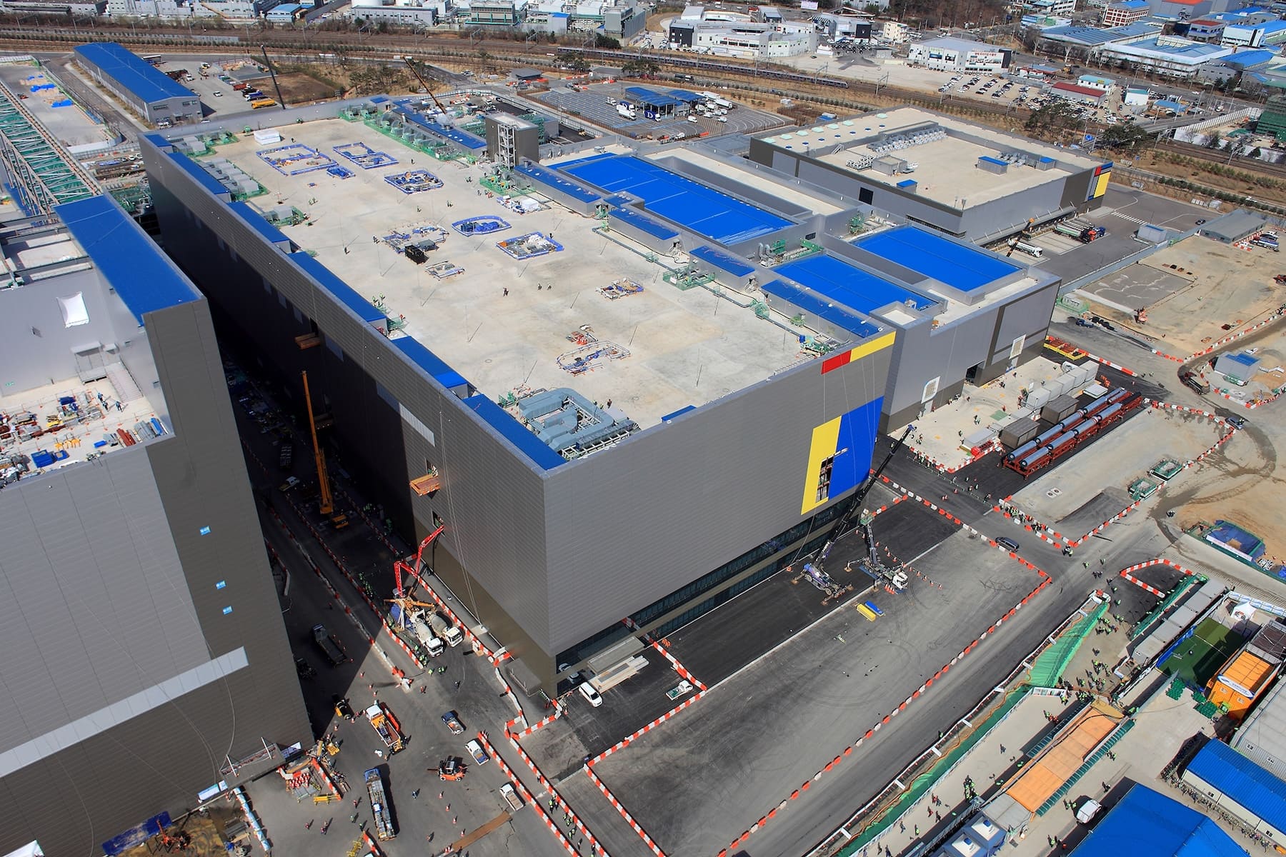
Samsung is starting to leave behind one of its biggest headaches in semiconductors. Its 4-nanometer manufacturing process, which for years struggled with performance issues and lost contracts to TSMC, has reportedly reached yield rates in the 60-70% range. This improvement is behind a new contract worth over $100 million with U.S.-based Tsavorite Scalable Intelligence, a company specializing in artificial intelligence.
According to information released by South Korean media, Samsung Foundry will manufacture an OPU (Omni Processing Unit) for this firm—a chip that combines CPU, GPU, and memory in a single package, designed for next-generation AI workloads. The order is estimated to be around 150 billion won, just over $100 million, and will be produced using the company’s 4 nm process.
From “Nightmare” to Strategic Asset
The 4 nm node has been a sensitive point in Samsung Foundry’s strategy for years. Initial low yields, well below expectations, led key customers to shift some of their designs to TSMC, the market leader, eroding confidence in Samsung’s ability to compete in advanced processes.
However, the situation is changing. Yields at 4 nm are now believed to have stabilized around 60-70%, a significant jump that transforms a previously unprofitable process into a viable platform for high-volume commercial products. For a customer like Tsavorite Scalable Intelligence, which aims to rapidly scale its compute capacity with proprietary AI chips, using a “not top-of-the-line” but more mature node makes economic sense:
- The cost per wafer is lower than at 3 nm or 2 nm,
- Yields are now reasonable,
- And the energy efficiency of the node remains competitive for many AI architectures.
What is an OPU and Why It Matters for AI
The chip Samsung will produce for Tsavorite is described as an Omni Processing Unit: a processor that integrates CPU, GPU, and memory into a single device, aimed at massively accelerating AI workloads.
This design seeks to reduce traditional bottlenecks between memory and computation—a major current limitation in AI chips. By bringing memory closer to the compute element (or even integrating it on the same die), latencies are reduced, and energy efficiency is improved—critical factors for data centers running large generative AI models or inference systems at scale.
That a project like this is being manufactured on 4 nm, rather than only in cutting-edge nodes like 3 nm or 2 nm, confirms a clear market trend: not all AI workloads require the most advanced node; many companies prioritize a balance between cost, performance, and manufacturing capacity availability.
A “Small” but Symbolic Contract
An order of just over $100 million may be relatively modest for Samsung’s overall size. But within its foundry business, it carries significant symbolic weight:
- It reinforces the idea that the 4 nm node has moved past the critical phase.
- It shows that AI clients are beginning to trust Samsung for advanced projects.
- It coincides with other significant contracts, such as autonomous driving chips for Tesla and orders from Chinese cryptocurrency mining equipment manufacturers.
These movements align with the company’s stated goal: to make its foundry business clearly profitable and turn it into a profit pillar by 2026-2027, at a time when demand for AI chips, HBM memory, and advanced nodes continues to grow.
The Ripple Effect of HBM4 and 2 nm
The rebound of 4 nm is not occurring alone. Samsung is also preparing for a crucial leap in high-performance memory: mass production of HBM4 starting in 2026. A key part of this roadmap is the so-called base die of HBM4, which will also be manufactured using the 4 nm process within Samsung’s foundry division.
This means that the same node previously considered problematic is now becoming the engine that fuels two expanding major businesses:
- HBM4 memory, essential for next-generation AI GPUs.
- Dedicates AI compute chips, such as Tsavorite’s OPU or chips for Tesla and other clients.
Meanwhile, Samsung continues to push its most advanced processes. The company has announced details of its first 2 nm node using GAA (Gate-All-Around) technology, promising performance and efficiency improvements over the second-generation 3 nm. Though the actual volume and initial customers for this node are yet to be confirmed, the message is clear: Samsung aims to challenge TSMC’s leadership in the 3 nm and 2 nm segments, while consolidating 4 nm as a mature and cost-effective alternative.
Tension on TSMC and the End of the “De Facto Monopoly”
The environment also favors Samsung. The strong demand for AI chips has strained TSMC’s capacity, especially on its most advanced nodes. Major customers like NVIDIA, Qualcomm, and automakers are feeling the physical limitations of available manufacturing capacity.
In this context, any competitor capable of offering:
- a sufficiently mature node,
- relevant production capacity,
- and competitive prices,
becomes an attractive alternative. Samsung is positioning itself not as a total replacement for TSMC, but as a second major supplier for large AI, automotive, and mobility projects.
Industry sources suggest that the current model, with TSMC accounting for about 70% of advanced foundry market share, may be unsustainable long-term if demand for AI chips continues to grow. Any advances Samsung makes in key processes like 4 nm could open opportunities to rebalance the semiconductor manufacturing landscape.
A Turning Point… if Future Chips Live Up to Expectations
The Tsavorite contract and the stabilization of 4 nm don’t guarantee Samsung Foundry’s definitive comeback, but they may mark a turning point. The real test will come with:
- The real performance of Tsavorite’s OPUs,
- Adoption of Samsung-manufactured HBM4 in upcoming AI GPUs,
- The reception of future 2 nm SoCs among major clients.
If these products meet expectations in performance, power consumption, and availability, South Korea’s Samsung could narrow the gap with TSMC—especially in the segment shaping the next decade: chips for artificial intelligence.
Source: AjuNews