The race to scale artificial intelligence is pushing the semiconductor industry into territories that just a few years ago seemed like science fiction. The latest move comes from South Korea: according to information published by specialized media, Meta and NVIDIA are studying integrating GPU cores directly into next-generation HBM memory, in collaboration with SK Hynix and Samsung Electronics.
If this architecture materializes into commercial products, it could fundamentally change how chips for AI data centers are designed and further blur the line between memory and processor.
What is HBM and why is everything centered around it
High Bandwidth Memory (HBM) is a type of memory created to solve a very specific problem: the lack of bandwidth between the processor and RAM in high-performance systems. Instead of placing memory chips around the GPU or CPU, HBM stacks multiple layers of DRAM on top of each other and connects them using TSV (Through-Silicon Vias), channels that traverse the silicon vertically.
These memory stacks are then mounted onto a silicon interposer next to the processor, in a packaging commonly referred to as 2.5D. The result is a compact module that offers:
- Much higher bandwidth than traditional GDDR or DDR memory.
- Lower energy consumption per bit transferred.
- Smaller physical footprint around the main chip.
For all these reasons, HBM has become the reference memory for AI GPUs, compute accelerators, and some high-performance processors. The latest developments, such as HBM3E and HBM4, push this idea further by increasing the number of layers, communication buses, and frequencies to surpass the threshold of terabytes per second per memory stack.
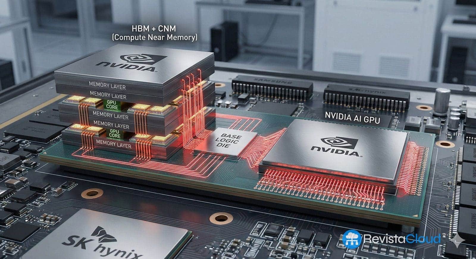
From “simple” controllers to GPU cores inside HBM
In the current architecture, HBM essentially stores data and serves it as rapidly as possible to the external processor. The logical component at the bottom of the stack, known as the base die, mainly manages communications between the memory layers and the rest of the system.
With HBM4, there’s a first change: some manufacturers are beginning to integrate more advanced memory controllers and additional logic into that base die. This logic optimizes how data is sent and received, reduces latencies, and improves efficiency without modifying the main chip.
The proposal now being discussed goes several steps further. According to information leaked from Korea, Meta and NVIDIA are evaluating integrating GPU cores into the base die of HBM, transforming that component into more than just a memory manager.
In practice, this would mean that part of the computing capacity that currently resides solely in the GPU would shift to the memory stack itself. The integrated GPU cores would be capable of executing operations directly on data without physically moving it to the main processor.
Why bringing computation closer to memory could change AI
In large AI data centers, a significant portion of energy consumption and bottlenecks is not so much due to computation itself, but to the constant data movement between memory and processor. Each transfer involves latency and energy expenditure.
The idea of integrating GPU cores into HBM specifically addresses this problem:
- Less physical distance between where data is stored and where it is processed.
- Less traffic over links between HBM and the main GPU.
- The ability to perform simple or repetitive operations directly in memory, leaving more complex tasks to the central GPU.
Sources from the industry cited by Korean media emphasize that in AI, it’s no longer just about “going faster,” but about improving energy efficiency per operation. Reducing a few nanoseconds of latency and a few watts per accelerates, multiplied across tens of thousands of nodes in a data center, can result in billions in savings and lessen the load on the electrical grid.
Technical challenges: space, energy, and heat in the base die
The theory is attractive, but implementing it in practice is not trivial. The HBM base die faces several key limitations:
- The manufacturing process with TSV leaves little free space for additional logic. Much of the surface area must be reserved for the vertical interconnections that link the layers.
- A GPU core, even small, consumes energy and generates heat. Integrating multiple cores beneath a stacked DRAM face challenges in power delivery and especially in thermal dissipation.
- The current 2.5D packaging is already complex; adding logic to the base die necessitates redesigning the interposer, power distribution networks, and cooling solutions.
If integrated cores consume too much energy or overheat, they can negatively impact the memory itself, reducing reliability or lifespan. Balancing added compute capacity and system stability will be a critical aspect of this architecture.
Meta, NVIDIA, SK Hynix, and Samsung: alliances breaking traditional boundaries
The fact that Meta, NVIDIA, SK Hynix, and Samsung Electronics are involved illustrates how much the sector landscape is shifting. Traditionally:
- Memory companies (SK Hynix, Samsung, Micron) focused on DRAM and NAND.
- Logic companies (NVIDIA, AMD, Intel, Qualcomm) designed GPUs, CPUs, and SoCs.
The idea of integrating GPU cores within HBM forces close collaboration: it requires cutting-edge expertise in both memory and logic, as well as advanced foundry and packaging capabilities.
For South Korean industry, this is a mix of opportunity and risk. If companies like SK Hynix and Samsung succeed in expanding their role beyond pure memory and become key partners for these hybrid solutions, they could claim a central position in the AI era.
However, if they fail to leap into logic design and the “custom HBM” ecosystem, they might end up subordinated to major system designers, who would use their manufacturing capacity as just another piece of a puzzle controlled externally.
“The boundary between memory and logic is vanishing”
Academic experts from institutions like the KAIST (Korea Advanced Institute of Science and Technology) highlight a clear trend: the boundary between memory and system is rapidly blurring as AI becomes more demanding.
The core message is that memory manufacturers can no longer limit themselves to improving density and speed; they must also venture into logic, offer joint solutions, and be part of an ecosystem ranging from accelerator design to advanced packaging and software.
In this context, discussions about HBM with integrated GPU cores are not an eccentricity but a sign of a new era: memory ceases to be a “passive” component and instead becomes an active contributor to computing.
HBM4, “custom HBM,” and the path toward memory-based computing
The standardization of HBM4 and the first commercial announcements from manufacturers like SK Hynix and Samsung point in this direction already. The new generation of HBM features:
- Interfaces up to 2,048 bits and projected speeds exceeding terabytes per second of bandwidth per stack.
- More complex base dies capable of integrating advanced memory controllers and custom logic tailored to the client.
- Packaging techniques such as MR-MUF or NCF+TCB, aimed at improving thermal and mechanical integrity of 12 or 16-layer stacks.
On this foundation, the concept of “custom HBM” is built — HBM4 memories designed specifically for a particular accelerator, with the base die tailored to the main chip’s needs. Incorporating GPU cores would be a further step in a trend already underway: moving more intelligence into memory itself.
What it could mean for the future of AI chips
Should Meta and NVIDIA, along with their memory partners, overcome technical barriers and bring to market HBM with integrated GPU cores, the implications could be profound:
- New category of accelerators: GPUs or XPUs where some calculations happen directly under the memory, breaking down the “memory wall” that currently limits many systems.
- Greater market fragmentation: each major cloud provider might commission its own customized combination of accelerator + HBM, complicating entry for smaller players.
- Additional pressure on the supply chain: advanced logic processes for base dies, TSV capabilities, and state-of-the-art packaging and tight coordination between foundries and memory makers will be necessary.
Simultaneously, this movement would reinforce the strategic importance of HBM as a critical resource for AI, strengthening the position of the few countries and companies capable of producing it at scale.
For now, the integration of GPU cores into HBM remains in the study and discussion phase. Yet, the very fact that names like Meta, NVIDIA, SK Hynix, and Samsung are exploring it indicates that the race to break the memory barrier has entered a much more aggressive stage.
FAQs about HBM with integrated GPU cores
What benefits would integrating GPU cores directly into HBM memory provide for AI?
The main benefit would be reducing the data movement between memory and processor. By executing some operations directly within the HBM’s base die, latency and energy consumption associated with data transfers decrease. This is especially critical in AI data centers, where models are enormous and workloads continuous. Improving efficiency per watt has a significant economic and operational impact.
How does HBM4 with an integrated controller differ from the proposal to add GPU cores?
Integrating a memory controller into HBM4 aims to optimize how reads and writes are managed, but its primary function remains storing and serving data rapidly. Adding GPU cores goes beyond management — enabling active computation directly on the data without removing it from the stack. These are two different levels of integration: first smarter management, then actual compute capability.
What technical challenges exist to embedding a GPU within HBM?
The main challenges are limited space in the base die due to TSVs, power supply for cores with high consumption, and heat management within a stacked DRAM. Excessive heat could damage memory or reduce reliability. Additionally, packaging and cooling become more complex, requiring innovative design solutions and materials.
How could this trend impact the semiconductor industry in Korea and globally?
For companies like SK Hynix and Samsung, integrating logic into HBM presents a major opportunity to evolve from memory suppliers to central players in AI chips. However, it also carries risk; those unable to combine memory, logic, and advanced packaging may become subordinate to large accelerator designers. Globally, this convergence underscores the strategic significance of the HBM supply chain and intensifies competition over controlling both memory production and advanced logic.
Sources:
– Information published by ETNews about Meta and NVIDIA’s plans to integrate GPU cores into HBM base dies with SK Hynix and Samsung.
– Technical documentation and industry announcements concerning HBM3E and HBM4, from JEDEC and manufacturers like SK Hynix, Samsung, and Micron.
– Sector analyses on high-bandwidth memory, 2.5D packaging, and trends in “compute near memory” and “compute under memory” for AI accelerators.