Tesla has cleared up the uncertainty: its upcoming autonomous driving chips, AI5 and AI6, will be manufactured in parallel at Samsung and TSMC, with slightly different physical versions but identical software behavior, as Elon Musk has confirmed. This move consolidates a dual-supplier strategy to secure volume, mitigate yield risks, and negotiate capacity in a market where the demand for AI silicon exceeds supply.
The announcement corrects the impression left by Musk himself in late October when he suggested that the Samsung plant in Taylor (Texas) had equipment “slightly more advanced” than TSMC in Arizona (Fab 21), implying a possible single fab approach for Tesla’s most ambitious chip. Ultimately, the plan is dual starting with AI5 and maintaining AI6, which promises to double performance compared to its predecessor while using the same manufacturers.
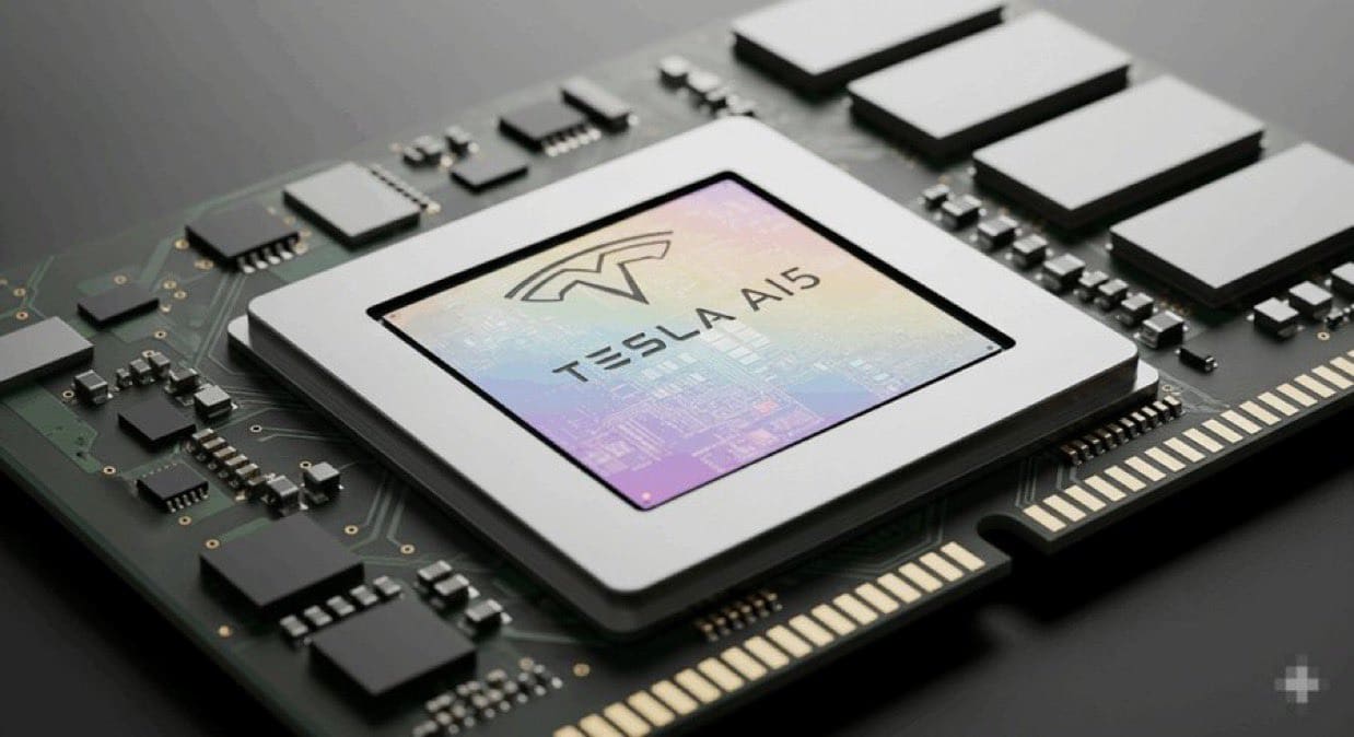
What does “two fabs, one chip” mean?
In semiconductor manufacturing, dual-sourcing is common: major customers often diversify to guarantee timelines and volumes. Musk explained that Samsung and TSMC interpret the same logical design differently in silicon, resulting in physical versions of AI5 (and later, AI6). The key, he insists, is that Tesla’s software runs the same on both, without any changes for the driver or the fleet.
Besides securing supply, this strategy offers industrial margins: if one foundry faces capacity strain, the other fab can take on part of the plan; and it allows Tesla to balance cost, performance, and schedule across two nodes and two different packaging lines.
Performance: ambitious promises (without public metrics)
During the Q3 earnings presentation, Musk stated that AI5 will be “40 times” better than AI4 (“not 40% but forty times”), though he did not specify metrics: it could refer to throughput, latency, energy efficiency, or a combination of several. He also mentioned AI6 as a “fast follow”— roughly 2× AI5— with Samsung and TSMC remaining as fabrication partners.
In the absence of detailed technical sheets, it’s best to consider these figures as targets. Recent information points to AI5 having a tape-out pending and production scheduled for 2026, although industry analysis suggests that mass production could shift to 2027, which is typical for projects of this scale. The dual foundry approach is precisely meant to mitigate those risks.
Why is this good for Tesla (and its AI roadmap)?
The scope of these chips extends beyond FSD. Musk envisions AI5/AI6 powering the Optimus humanoid robot and other emerging systems, so a high volume demand will be key. Relying on a single fab in the U.S. carries risks (capacity, timelines, and cost). With Samsung Taylor and TSMC Arizona operating in parallel, Tesla gains resilience:
- Capacity: more wafers potential in a market stressed by generative AI.
- Negotiation: greater bargaining power for pricing and allocations.
- Schedule: reduced bottleneck risk if one plant faces adjustments or slower ramp-ups.
On a technical level, Tesla aims to abstract process and packaging differences to deliver a unified execution platform across the fleet, regardless of where the chip was fabricated.
Will this displace Nvidia? It’s still early
Musk has claimed that the new generation will be much cheaper and more efficient than reference GPUs on the market. Without official documentation, it’s prudent to contextualize: Tesla designs custom ASICs for its loads (perception, planning, control), whereas Nvidia produces general-purpose GPUs aimed at training and inference of diverse models. It’s not a “one-to-one” comparison. If Tesla manages to multiply performance per dollar in its domain, it will reduce external dependency in the edge inference of vehicles and robotics; but verification will depend on actual silicon and public benchmarks.
Tentative timeline
- AI5: in development; tape-out pending; targeted 2026 production with initial deployments subject to yield ramp.
- AI6: approximately 12 months later; aiming for roughly 2× AI5 while maintaining Samsung/TSMC; schedule for 2027/2028 depending on ramp-up.
- AI7: Musk describes as “more adventurous”; might switch nodes and partners, but no details yet.
What to watch moving forward
- Node and packaging: whether AI5/AI6 use advanced nodes from the U.S. (Arizona/Texas) and which interconnection technologies they adopt (CoWoS, I-Cube, SoIC, etc.).
- Yield and costs: balancing process maturity (TSMC) and latest equipment (Samsung Taylor).
- Functional parity: whether the software abstraction ensures both variants perform equivalently fleet-wide.
- Time to volume: whether the actual ramp confirms 2026–2027 or gets closer to 2027–2028.
Frequently Asked Questions
Why manufacture AI5/AI6 at Samsung and TSMC simultaneously?
To secure capacity, redund against possible yield problems, and accelerate the transition from prototype to volume. For critical, high-demand chips, dual-sourcing is standard practice.
Will there be differences between Samsung and TSMC versions?
Yes, physically (due to how each foundry translates the design to silicon), but the goal is that software and actual performance are equivalent. Tesla validates this parity within their AI stack before deployment.
When will AI5 and AI6 reach production?
Musk targets AI5 in 2026 and AI6 about a year later; industry analysis considers 2027 for mass production. It’s normal for schedules to shift until the chips ramp on the chosen node.
Will this displace Nvidia?
Not necessarily. Tesla competes with ASICs specialized for its stack; Nvidia dominates training and general inference. They occupy complementary spaces. Tesla’s key will be achieving promised performance per watt and cost per inference in field.
via: tomshardware