SK hynix has unveiled its most ambitious roadmap to date during the SK AI Summit 2025. This is not just a simple schedule of more layers and higher MHz; it’s a AI-centric vision encompassing high-bandwidth memory (HBM), conventional DRAM, NAND/SSD, and new “smart” blocks promising to take computing beyond the memory wall. The company divides it into two stages with very clear objectives:
- 2026–2028: Aggressive deployment of HBM4/HBM4E and the introduction of LPDDR6; DRAM optimizations aimed at reducing total costs in datacenter; transition to PCIe 6.0 in SSDs.
- 2029–2031: Consolidation and a new wave featuring HBM5/HBM5E (standard and custom), DDR6, GDDR7-Next (the foundation of future GDDR8), 3D DRAM, PCIe 7.0 in SSDs, UFS 6.0 in mobile devices, and NAND 4D with more than 400 layers.
Along the way, two key concepts emerge, running across all product families:
- AI-D (AI-DRAM): optimization, breaking through the memory wall, and expansion into new segments with CXL, PIM (in-memory processing), and formats like MRDIMM or SOCAMM2.
- AI-N (AI-NAND/Next Storage): SSDs and memories aware of AI workloads, prioritizing performance, bandwidth, or density depending on the case.
Here are the puzzle pieces and why they matter.
AI-N: three “profiles” of storage for the AI era
During the opening of the presentation (“New Vision & New Technology in AI Era”), SK hynix grouped the storage of tomorrow into three profiles, all under the AI-N umbrella:
- AI-N Performance (Storage Next): SSD optimized for high performance. The company showed a diagram with PCIe Gen6 eSSD access routes and a hierarchy where the SSD is integrated into a low-latency fabric alongside CPU, GPU, HBM, and NIC. The idea: minimize I/O bottlenecks in token-intensive workloads and those with growing context windows.
- AI-N Bandwidth (HBF – High Bandwidth Flash): a high-bandwidth flash SSD with TSV. The technical scheme reflects TSV and microbumps on a base die, connecting flash matrices with vertical interconnections to boost throughput over a conventional eSSD. The goal is to approach — with NAND costs — the rates demanded by massive training and inference.
- AI-N Density (NLF & NL SSD): Very high-capacity NAND and low-cost SSD for mass storage. In the hierarchy pyramid (HDD→NL SSD→QLC/TLC SSD→DRAM→HBM), this category pushes capacity upward with reduced cost per bit, feeding data lakes and datasets repositories that grow uncontrollably.

Practical translation: The company doesn’t see a single “AI-SSD,” but families of specialized ones —performance, bandwidth, or density— that will combine in AI-native datacenters.
Standard HBM vs. custom HBM: reconfiguring components to save power and gain compute area
Another key part of the presentation opposes standard HBM with custom HBM. In conventional design, many interface blocks (PHY/controllers) are split between the base HBM die and the SoC/GPU. The “Custom HBM” proposal relocates functions:
- In the base HBM die, HBM Controller and a D2D PHY (die-to-die) are integrated.
- In the SoC/GPU, the pathway to HBM is reduced to a lighter D2D PHY.
The outcome, according to SK hynix: more area available for compute cores on the host chip and lower power consumption in interfaces. This points towards a market where memory and compute are co-designed (DTCO→STCO), especially in AI accelerators.
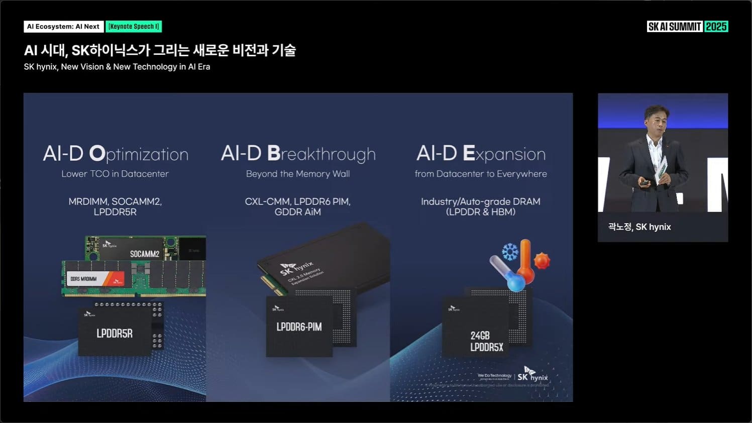
AI-D: optimization today, breaking the memory wall tomorrow
Under the AI-D (AI-DRAM) brand, SK hynix structures its DRAM strategy around three axes:
- Optimization (Lower TCO in Datacenter)
- MRDIMM, SOCAMM2, and LPDDR5R aim to reduce total cost and consumption in rack data centers. MRDIMM targets higher bandwidth per module, and SOCAMM2 aims for density in compact form factors.
- Breakthrough (Beyond the Memory Wall)
- CXL-CMM (memory poolable and coherent via Compute Express Link), LPDDR6-PIM (in-memory processing), and GDDR AiM (in-memory acceleration). The goal is to shift computing (reduce, search, scatter/gather) closer to the data, easing pressure on buses and controllers.
- Expansion (From Datacenter to Everywhere)
- Industrial/automotive-grade DRAM (LPDDR/HBM) and LPDDR5X/LPDDR6 in devices and edge computing, enabling AI to extend beyond data centers without sacrificing reliability.

Practical translation: SK hynix extends its DRAM roadmap, aiming to lead advances in performance, power efficiency, and density across data centers, mobile, and edge devices, with significant milestones in the coming years.
The schedule: 2026–2028 (deployment) and 2029–2031 (new wave)
The final slide summarizes the roadmap in four vertical lines (HBM, conventional DRAM, AI-D DRAM, NAND). These are the visible milestones:
2026–2028
- Standard HBM: HBM4 16-Hi; HBM4E in 8/12/16-Hi.
- Custom HBM: Custom HBM4E for AI and supercomputing clients.
- Conventional DRAM (standard): LPDDR6 as the new standard in mobile/laptop.
- AI-D: LPDDR5X in SOCAMM2, MRDIMM Gen2, LPDDR5R; 2nd gen CXL, and initial LPDDR6-PIM.
- NAND (standard): PCIe Gen5 eSSD (target capacities reaching over 200+ TB in QLC in public roadmaps), progressing to PCIe Gen6 eSSD/cSSD and UFS 5.0 in mobile devices.
- NAND (AI-N): initiation of AI-N D (density-oriented families with predictive data management).
Implication: A broad deployment of HBM4/4E for training and inference of frontier models, mobile devices with LPDDR6, and SSD PCIe 6.0 as the backbone in new racks. CXL convergence begins, and early PIM products appear.
2029–2031
- Standard HBM: HBM5 and HBM5E.
- Custom HBM: custom variants of HBM5/HBM5E.
- Conventional DRAM (standard): GDDR7-Next (foundation of future GDDR8), DDR6, and 3D DRAM.
- AI-D: LPDDR6 on SOCAMM2 (expansion), 3rd gen CXL, and PIM-Next (next-generation memory computing).
- NAND (standard): PCIe Gen7 eSSD/cSSD, UFS 6.0, and NAND 4D with 400+ layers.
- NAND (AI-N): AI-N P (Storage Next) and AI-N B (HBF) mature, bringing bandwidth and AI optimization to the forefront.
Implication: A new wave pairing HBM5 with next-generation accelerators, bringing DDR6/ GDDR7-Next to PCs and gaming. Storage advances include PCIe 7.0 in datacenters, UFS 6.0 in mobile, and NAND 4D breaking the 400-layer barrier.
Implications: AI, gaming, mobile, and edge
- Frontier training and inference: HBM4E→HBM5 and HBF (flash with TSV) will expand the data pipeline from SSD to GPU/ASIC, reducing bottlenecks in token-heavy pipelines and long-context scenarios.
- PC and gaming: GDDR7-Next and DDR6 will boost bandwidth and latency; the mention of 3D DRAM hints at vertical stacking for higher densities.
- Mobile and edge: LPDDR6 as a baseline, UFS 6.0 in the latter half of the decade, and LPDDR6-PIM for local inference with lower power; automotive and industry applications with specific grade DRAM.
- Memory-centric architectures: CXL (Gen2→Gen3) enables shared pools of memory and decoupled expansion; PIM and AiM (accelerated-in-memory) bring operations closer to the data, key to reducing p99 latency.
- Sustainability: although no PUE/WUE figures were shown, the shift to HBM5/HBM5E and custom HBM suggests power reduction in interfaces and an improved compute area per die—two critical factors in the energy consumption of AI racks.

What makes this roadmap different
- Memory as a system, not just as a component: custom HBM, CXL, PIM, and AiM point to co-design with CPU/GPU/ASICs.
- AI-aware storage: AI-N separates profiles (Performance/Bandwidth/Density) and anticipates high-bandwidth flash (HBF) with TSV.
- Long-term, coherent calendar: the vision extends to 2031, connecting families (HBM, DRAM, NAND) with clear cross points between stages.
If SK hynix achieves this, it will not just keep pace with AI but may set the pace and influence designs of accelerators, servers, and endpoints for the coming decade.
What to watch from 2026 onward
- HBM4E 16-Hi in commercial accelerators and the adoption of custom HBM (power and area savings).
- Latencies and throughput of HBF compared to conventional PCIe 6.0 eSSD.
- Second-generation CXL in production (added latency, software stack, and orchestration).
- First demos of LPDDR6-PIM and GDDR AiM in real use cases (filtering, reduce, searches).
- Density evolution in NAND 4D towards the anticipated 400+ layers for 2029–2031.
FAQ
When will SK hynix release HBM5 to the market?
In the second phase of the roadmap, between 2029 and 2031. SK hynix plans HBM5 and HBM5E in both standard and custom forms, targeting AI accelerators and next-gen GPUs.
What is HBF (High Bandwidth Flash), and how does it differ from a conventional SSD?
HBF is a concept of high-bandwidth Flash utilizing TSV and microbumps to increase throughput compared to standard PCIe eSSD. It does not replace HBM but brings storage closer to the speeds required for large-scale training and inference.
Which DRAM technologies will we see between 2026–2028 and after 2029?
Between 2026 and 2028: LPDDR6 as the new standard, MRDIMM Gen2, SOCAMM2, CXL Gen2, and initial LPDDR6-PIM. From 2029 onward: DDR6, GDDR7-Next (foundation for GDDR8), 3D DRAM, CXL Gen3, and PIM-Next.
What does SK hynix’s storage roadmap beyond 2028 entail for mobile and datacenter?
For datacenters: PCIe Gen7 eSSD/cSSD and NAND 4D with 400+ layers in 2029–2031. For mobile: UFS 6.0 and continuity of LPDDR6 as standard memory, with PIM and AI-N variants focused on density and efficiency.
Sources
- SK AI Summit 2025 – Presentation “AI Ecosystem: AI Next | SK hynix, New Vision & New Technology in AI Era” (keynote slides featuring AI-N, AI-D, comparison of standard vs. custom HBM, and roadmap 2026–2031).
- Official visual materials from SK hynix shown during the conference (screenshots provided).