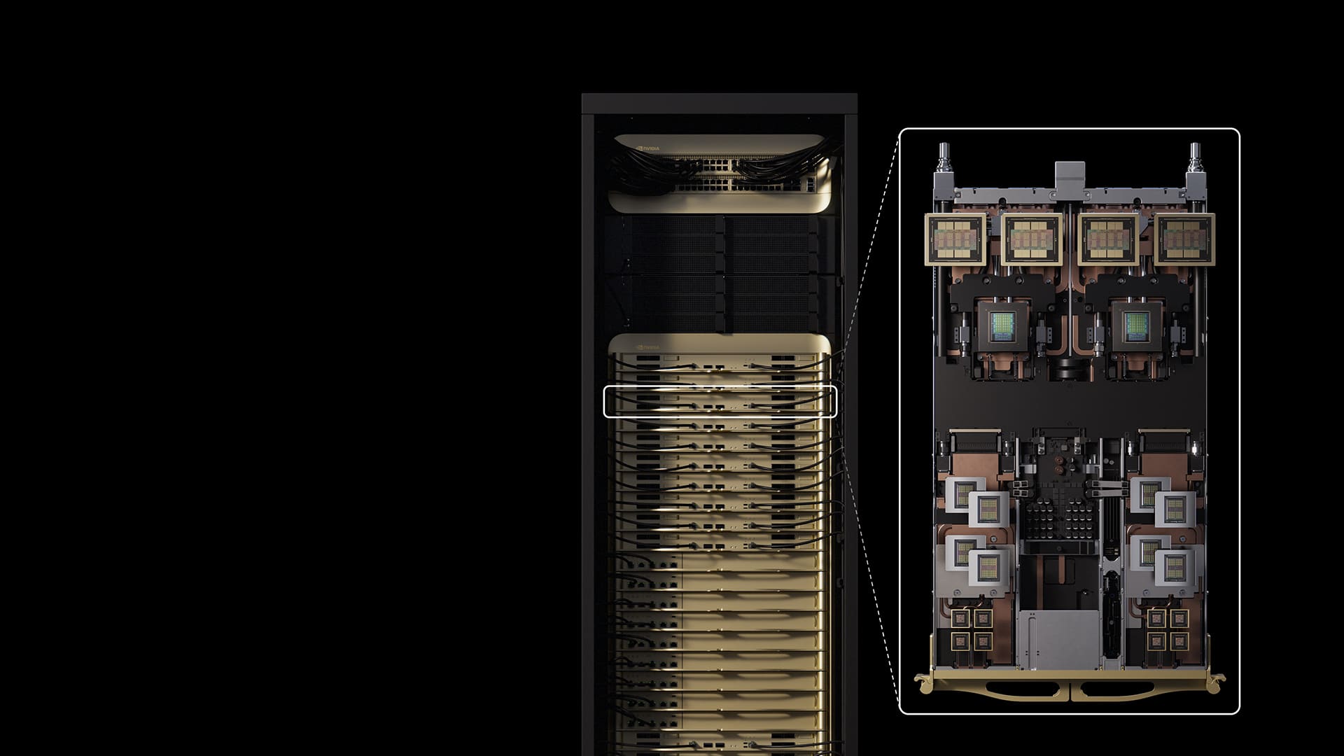
NVIDIA has publicly unveiled its Vera Rubin Superchip, the platform that will mark its next big leap in AI computing following Blackwell. On the stage at GTC Washington (October 2025), Jensen Huang showcased an actual board integrating two Rubin GPUs and an 88-core Vera CPU (176 threads), interconnected via NVLink-C2C at 1.8 TB/s, complemented by onboard ‘fast’ memory (LPDDR) reaching 2.0 TB in the demo, along with HBM4 on each GPU. According to the shared roadmap, the first Rubin units are already in NVIDIA laboratories, with volume production expected to begin late 2026 (mid to late Q4), parallel to the rollout of Blackwell Ultra (GB300).
The company also introduced two reference systems designed to standardize Rubin in data centers: NVL144 (2026) and Rubin Ultra NVL576 (2027), featuring notable improvements in compute, memory, and networking compared to the Blackwell generation.
What is the Vera Rubin Superchip (and why does it matter)
Vera Rubin embodies NVIDIA’s push towards “rack-scale” systems: CPU + GPU combined in a single superchip with high-speed interconnects, local LPDDR memory serving as “fast memory” for control and services, and HBM4 attached to each GPU to maximize bandwidth during training and inference. The Vera CPU employs 88 custom Arm cores (176 threads), acting as a close coordinator for the two Rubin GPUs, each composed of two reticle-sized chiplets.
In the GTC showcase, besides the dense power delivery surrounding the GPUs, multiple LPDDR memory modules for the CPU were visible, with the demo’s label highlighting “100 PF AI” and “2 TB Fast Memory,” clearly positioning the setup as a large-scale AI generative and agentic engine.
NVL144 (2026): 3.6 exaflops FP4 and upgraded interconnects
The inaugural system in this family will be Vera Rubin NVL144, scheduled for second half of 2026. Its technical specs include:
- Rubin GPU: two chiplets “reticle-sized” per GPU, offering up to 50 PFLOPS FP4 per accelerator and 288 GB of HBM4 per GPU.
- Vera CPU: 88 Arm cores / 176 threads.
- CPU-GPU link: NVLink-C2C at 1.8 TB/s.
- Performance: approximately 3.6 exaflops in FP4 (inference) and 1.2 exaflops in FP8 (training), about 3.3× the performance of GB300 NVL72.
- Memory bandwidth: combining 13 TB/s of HBM4 and approximately 75 TB of total “fast memory” at system level.
- Networking: NVLink up to 260 TB/s and CX9 up to 28.8 TB/s.
NVIDIA’s goal with NVL144 is providing an immediate ramp-up for entities standardizing on GB300 looking to double their compute density and bandwidth without overhauling their entire data plane.
Rubin Ultra NVL576 (2027): four chiplets per GPU, 1 TB of HBM4e, up to 15 exaflops FP4
Arriving in 2027, Rubin Ultra NVL576 scales the topology to 576 GPUs and doubles the number of chiplets per GPU:
- Rubin Ultra GPU: four reticle-sized chiplets, enabling up to 100 PFLOPS FP4 per accelerator and 1 TB of HBM4e per GPU (16 stacks).
- Platform performance: about 15 exaflops in FP4 (inference), and 5 exaflops in FP8 (training), roughly 14× over NVL72 GB300.
- Memory bandwidth: approximately 4.6 PB/s with HBM4 and around 365 TB of “fast memory”.
- Network throughput: up to 1.5 PB/s via NVLink and 115.2 TB/s over CX9, marking a generational leap in NVLink/NVSwitch.
Industry analyses estimate that the liquid-cooled rack configuration of NVL576 will consume about 600 kW, illustrating the thermal and electrical challenge of the next wave of large-scale AI superchips.
Integration with Blackwell (GB300) and what has changed
Blackwell Ultra (GB300) is the 2025 platform geared for accelerating generative AI workloads with HBM3e and marked advancements in FP4/FP8 over Hopper. Rubin advances this with HBM4/HBM4e, larger chiplets within reticle limits, enhanced interconnects and memory, plus an accompanying Arm CPU with large LPDDR capacity for services and coordination. Metrics show NVL144 delivers about 3.3× performance over GB300 NVL72, with Rubin Ultra multiplying performance by 14.
Expected coexistence is plausible: GB300 will continue to be produced and deployed through 2025-2026, while Rubin prepares in 2026 to handle peaks in training and massive inference tasks requiring even more bandwidth and memory.
Supply chain: HBM4 and production timelines
The specifics of HBM4/HBM4e are critical. Transitioning from HBM3e demands new stacks (wider/higher), new materials, and more demanding packaging, along with coordination with TSMC for interposers and major memory vendors. NVIDIA reports having received the first Rubin GPUs, with mass production targeted for late 2026, aligning with HBM4 validation and ecosystem timelines.
Risks and open questions
As with any future-oriented presentation, the figures are targets: as HBM4 and chiplets mature, expect adjustments in frequencies, power consumption, and performance (yield). Details are still pending on supported FP modes (FP4/FP8/BF16/FP16) and the precise memory allocation between LPDDR and HBM per configuration.
The GTC demo clarifies the general direction: more memory, higher bandwidth, increased density per rack, with CPU–GPU integration and NVLink as the “nervous system” of this new architecture.
Frequently Asked Questions
What sets Rubin apart from Blackwell?
Rubin introduces HBM4/HBM4e, larger multi-chiplet GPUs within the reticle, an integrated Vera Arm CPU (88 cores), and NVLink-C2C at 1.8 TB/s between CPU and GPU. Compared to GB300, NVL144 scales approximately 3.3× in FP4/FP8, with Rubin Ultra reaching up to 14× over NVL72.
What do “exaflops FP4/FP8” mean?
They measure performance units in low-precision floating point (FP4/FP8), used primarily for generative AI: FP8 is typically employed during training; FP4, during large-scale inference. They are not directly comparable 1:1 to traditional FP64 HPC units.
When can Rubin be purchased?
NVIDIA anticipates mass production by late 2026. Systems based on NVL144 are expected in second half of 2026, and Rubin Ultra NVL576 in second half of 2027. Actual deployment depends on HBM4 validation, platform readiness, and manufacturing capacity.
What is the role of the 2.0 TB “fast memory”?
It’s LPDDR on board, linked to the Vera CPU, serving services, coordination, and close control tasks near the GPU. It does not replace the HBM4 powering the intensive compute but helps reduce latencies and alleviates data access to non-resident HBM data.
Sources (selected):
Preliminary coverage and specs of the Vera Rubin Superchip, NVL144 (2026), and Rubin Ultra NVL576 (2027); first hardware images at GTC Washington 2025; details on Vera CPU (88 Arm / 176 threads), HBM4/HBM4e, NVLink-C2C 1.8 TB/s, and performance/memory/network goals.