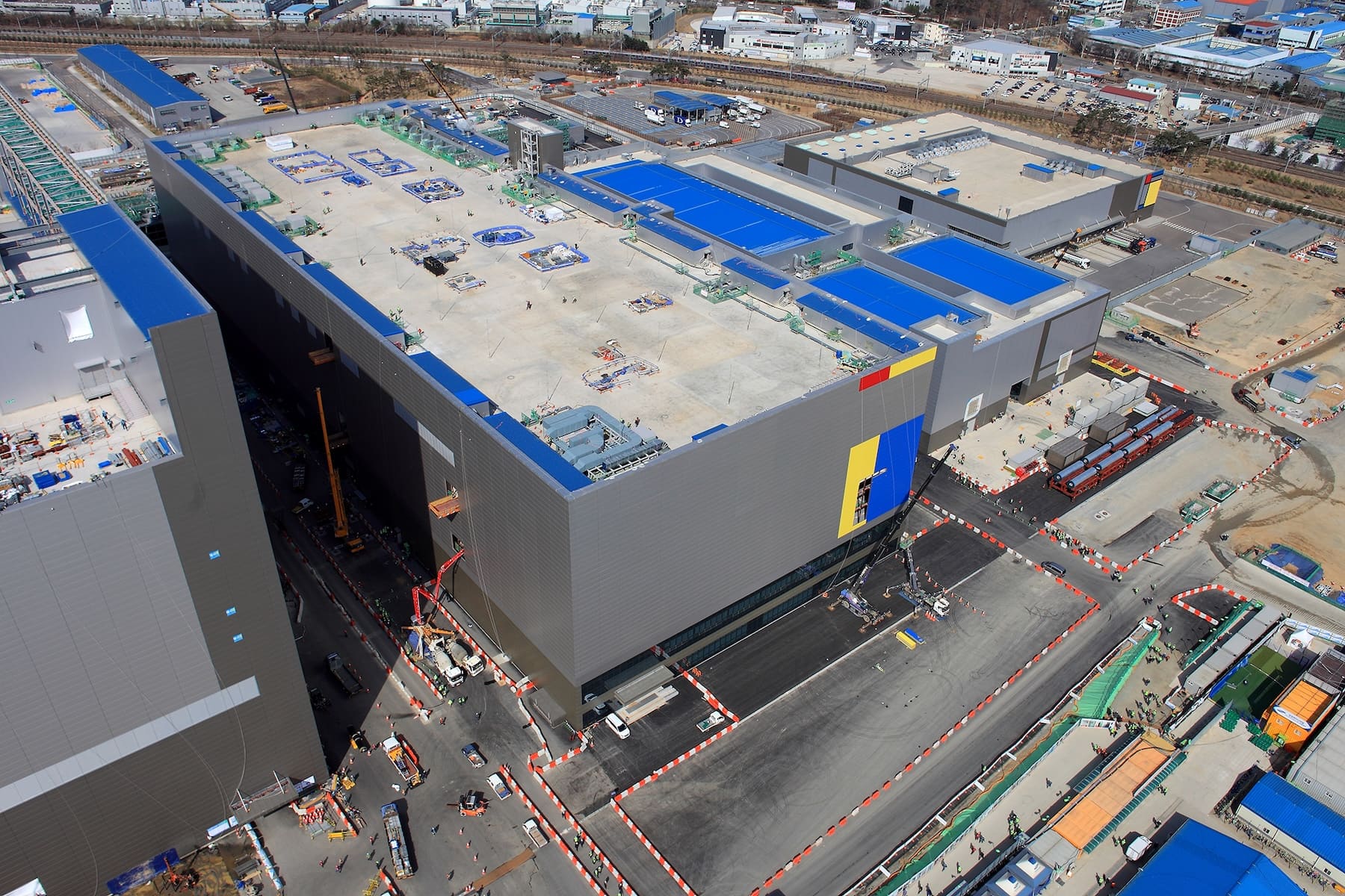
In an industry accustomed to measuring progress in nanometers and celebrating each node leap as a sign of speed and efficiency, Samsung Foundry has named the lever that, according to its executives, will make a difference in the next decade: DTCO (Design-Technology Co-Optimization), or joint optimization of design and process. During the 8th Semiconductor Industry-Academia Exchange Workshop held at COEX in Seoul as part of SEDEX 2025, Shin Jong-sin, Vice President of Samsung’s Foundry Division, argued that pure lithography scaling is no longer enough and that real improvement will come from co-designing chip architecture alongside process rules.
“With miniaturization alone, gains stay around 10-15%,” Shin warned. “As we push toward increasingly fine nodes, process improvements hit a ceiling, and industry is looking to DTCO to keep advancing.”
From “smaller is better” to “better-designed is better”
Samsung’s thesis starts from a growingly shared diagnosis: a node jump —from “N” to “M”, in industry jargon— no longer multiplies performance or reduces area as before. According to Shin, in practice, moving from one generation typically yields around 15% more performance and 15% less area, far from the 2× factors associated with the old “myth” of Moore’s Law. In this context, DTCO proposes breaking the traditional boundary between what the designer (architecture, cell libraries, interconnection topologies) determines and what the process (routing rules, metalization depth, power resources, pitch restrictions) enforces.
How does it work in practice? The design team defines functional requirements and bottlenecks, and process engineers adjust rules and stacks — from track width to cell height or the number of tracks per row — to enable new options, which in turn unlock better placement, shorter routes, or more efficient cells. This give-and-take allows, for example, condensing critical blocks, reducing interconnect capacitance, improving power distribution, and lowering power consumption without sacrificing timing.
Shin quantified the impact: at 7 nm, around 10% of the overall performance gain already came from DTCO. Below 3 nm, the company expects this contribution to scale up to 50%. It’s no coincidence that both Samsung and TSMC now have dedicated teams for this discipline, driven by the physics (quantum effects, variability, IR-drop, electromigration) and by an increasing demand — from AI — that grows at a pace that “doubles every few months”, while silicon node improvements lag at about 1-2% per revision.
From planar to FinFET and now GAA: the terrain where DTCO makes a difference
The executive reviewed the evolution of transistor architecture: from the classic planar to FinFET and more recently to GAA (Gate-All-Around), where the gate surrounds completely the channel to enhance electrostatic control and reduce leaks. Samsung prides itself on being pioneer in 14 nm FinFET and leading GAA to volume production, with billions of GAA transistors already integrated into devices like smartphones.
Specifically, GAA exemplifies how DTCO translates physics into design advantages. Unlike FinFET, the GAA structure allows manipulation of the number of “hilos” (nanolaminas/nanowires) and the cell height, opening the door to more flexible libraries. Samsung exploits this margin with what it calls “Hypercell”: customized larger cells in critical paths (to boost drive and meet timing) combined with more compact standard cells in less demanding zones. Overall area might grow slightly, but speed and energy efficiency improve, thereby raising ROI of the node without waiting for the next lithography leap.
It’s not all about P, A, and P: the “P” of Power Integrity is gaining importance
Another pillar that DTCO is reinforcing is power integrity (PI). Shin highlighted that power consumption profiles and power delivery network stability are now critical disciplines within foundries. Simulating the power mesh and current flow early in the design phase — when the design remains flexible — enables anticipating voltage drops (IR-drop), mitigating noise, and avoiding last-minute surprises, which otherwise would force over-dimensioning or frequency degradation. “Integrating PI work from the setup phase makes it more feasible to deliver an optimized chip that meets client demands,” he argued.
AI for better cell generation (and avoiding endless libraries)
South Korean foundry is also applying artificial intelligence to a traditionally craft-based task: cell generation. Traditionally, suppliers create thousands of cells (NAND, NOR, AOI, OAI, flip-flops, latches, drive variations, different heights), but only a fraction are used intensively. Shin explained that AI models analyze RTL synthesis results to identify common combinations and usage patterns, then produce “bespoke” composite cells. With these new pieces, a second Place & Route cycle can maximize area and power efficiency beyond what a generic library can achieve.
This approach aligns with the DTCO philosophy: instead of forcing design to fit process limitations, both sides — process rules and cell offerings — are modulated to optimally meet the actual circuit needs.
Beyond DTCO: toward SPCO and SDTCO
Shin concluded with a future outlook: what is now DTCO — design and process — will evolve into SPCO (System-Process Co-Optimization) and SDTCO (System-Design-Technology Co-Optimization), extending the co-design approach to the system level. In this vision, architecture, microarchitecture, libraries, interconnection, packaging (encapsulation), and even 2.5D/3D integration would be treated as a unified optimization space with shared rules and goals. This trend aligns with the market’s focus on heterogeneity — GPUs, NPUs, chiplets, HBM, chip-on-wafer-on-substrate — and customers demanding solutions (performance per watt, latency, cost per die, time-to-market), not just nodes.
The competitive landscape: everyone’s aiming at the same target
While the executive avoided direct references to competitors, he acknowledged that TSMC and Samsung maintain DTCO teams working closely with fabless clients and EDA providers. It makes sense: in a world where process milestones account for 10-15% gains per node, any 1-2% optimization — which might seem marginal elsewhere — decides contracts and feasibility. It’s in this margin where the art of aligning performance (P), power (P), and area (A) with deadlines and costs becomes a strategic advantage.
What can the ecosystem expect?
For chip designers, expanding DTCO means more interactive collaboration with the foundry and earlier iterations, but also fewer surprises at the end of the cycle. Custom libraries, routing rules tuned to actual topologies, and power meshes dimensioned with data can lower cancellation risks and rework.
For EDA vendors, the message is an invitation (and a challenge): to expose richer process models, automate design-process explorations, and close the loop with synthesis and P&R tools that speak the same language as the foundry.
For end customers — consumer electronics, hyperscalers, automotive, networking — the promise is concrete: faster, more efficient chips without waiting for a lithography miracle. In a market driven by AI — consuming memory and compute — exploiting every watt and millimeter might spell the difference between on-time launch or being sidelined.
Uncertainties: transparency, metrics, and timelines
Questions remain. How much transparency will there be in the “DTCO rules” that a foundry provides each client? How will the real contribution of DTCO to PPA be measured beyond marketing narratives? When will these improvements reach nodes below 3 nm? And most importantly, how will the balance evolve between pushing DTCO to the limit and maintaining porting of designs across different foundries?
Shin provided no specific product details or public roadmaps, but his message was clear: the competition at 3 nm and into the future sub-3 nm scale will no longer be settled solely in cleanrooms but also within design files, scripts, and libraries. For Samsung, DTCO is the name of that frontier.
Frequently Asked Questions
What exactly is DTCO (Design-Technology Co-Optimization), and how does it differ from traditional scaling?
DTCO is a co-design approach where design and process are adjusted together: layout rules, cell heights, track counts, power meshes, or cell libraries are reviewed to optimize PPA beyond what lithographic scaling alone achieves. Instead of “smaller is better,” DTCO advocates for “better thought is better.”
via: thelec.kr