Intel has named and scheduled its node leap: Panther Lake, the new Intel® Core™ Ultra 3 series for consumers, will be the first 18A SoC (a 2 nm class node developed and manufactured in the USA) and will enter high-volume production in Arizona by late 2025. The company also previewed Clearwater Forest (Xeon 6+)—its first 18A server—scheduled for the first half of 2026. Both will be produced at Fab 52 in Ocotillo (Chandler), the new pillar of Intel’s industrial plan in the U.S.
“We are entering a new era of computing thanks to advances in semiconductors that will shape the decades to come,” said Lip-Bu Tan, Intel’s CEO.
Panther Lake (Core Ultra 3): AI PC with multi-chiplet architecture, 18A, and up to 180 TOPS platform
Designed for consumer, enterprise, gaming, and edge/robotics, Panther Lake debuts a scalable multi-chiplet design that allows for multiple form factors and price points. Key highlights:
- Intel 18A node (2 nm class) featuring RibbonFET (new GAA transistor) and PowerVia (back-side power delivery) + Foveros (3D stacking) for integrating chiplets.
- CPU: up to 16 cores combining P-cores and E-cores; ≈ +50% CPU performance vs. previous gen (Intel estimates).
- GPU: new Intel® Arc™ with up to 12 Xe cores, ≈ +50% graphics performance vs. previous gen (according to benchmarks/titles specified by Intel).
- AI: a balanced XPU design (CPU+GPU+NPU) providing up to 180 TOPS platform performance.
- Efficiency: promises Lunar Lake-level efficiency with performance comparable to Arrow Lake.
- Edge robotics: reference board and Intel Robotics AI for integrating control + AI perception in a single SoC.
Schedule
- High-volume manufacturing (HVM) in 2025.
- Initial shipment (initial SKU) before the end of 2025.
- Broad availability in channels: January 2026.
Clearwater Forest (Xeon 6+): Dense, efficient, and in 18A for hyperscale
The E-core successor for data centers modernizes the Xeon family:
- Up to 288 E-cores per socket.
- ≈ +17% IPC vs. previous generation.
- Focus on density, performance per watt, and energy cost for cloud, hyperscale, and telco.
- Launch: 1H 2026.
Intel 18A: the “Made in USA” node with leadership ambitions
Intel positions 18A as its most advanced node developed and manufactured in the U.S., with internal metrics of:
- ≈ +15% performance per watt vs. Intel 3.
- ≈ +30% density vs. Intel 3.
Distinctive Technologies
- RibbonFET: Intel’s first GAA transistor in over a decade (better channel control and efficiency).
- PowerVia: backside wafer power delivery (reducing IR drop, cleaner signals).
- Foveros: 3D packaging for heterogeneous chiplets (flexibility, scalability, granular binning).
Roadmap
18A will serve as the foundation for at least three future generations in client and server segments (beyond Panther Lake and Clearwater Forest).
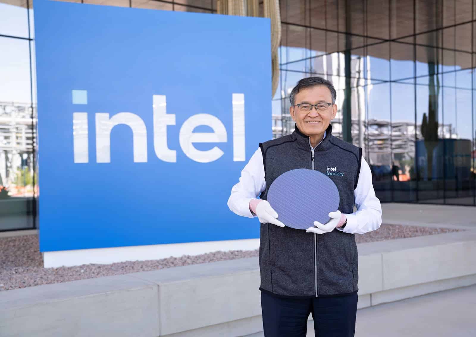
Fab 52 (Ocotillo, Arizona): domestic manufacturing and capacity for Intel Foundry
The Fab 52—the fifth high-volume factory on the campus—will be the HVM driver for 18A in the U.S. before year’s end. It’s part of the approx. $100B investment to expand R&D and domestic manufacturing (Oregon for R&D/early, Arizona for HVM, and New Mexico for packaging). The company emphasizes this supports U.S. strategic priorities and provides capacity for Intel Foundry customers in the AI era.
What it means for the market (and the PC)
- AI PC with leading node: bringing 18A to consumers aims for tangible differentiation (performance/efficiency/AI) against rivals relying on external nodes.
- XPU and chiplets: the chiplet flexibility allows more refined SKUs (performance, power, cost) and accelerates time-to-market.
- AI ecosystem: up to 180 TOPS platform performance supports local experiences (co-pilots, content creation, vision, translation) with less dependence on the cloud.
- Industrial signal: 18A HVM in the U.S. sends a message to fabless clients and advocates for industrial policy focused on supply chain resilience and process leadership.
Quick questions and answers
How does Panther Lake compare to Lunar/Arrow Lake?
Intel describes it as a “Lunar” efficiency chip with “Arrow” performance, adding AI XPU and a more powerful GPU Arc, all built on 18A and chiplets.
What to expect from the integrated GPU?
Up to 12 Xe and roughly +50% in gaming/benchmarks cited by Intel; the goal is to solidify 1080p e-sports, accelerate creator workflows, and support AI.
Does Xeon 6+ replace Granite/Sierra Forest?
It is the E-core leap in 18A for scale/efficiency workloads; it will coexist depending on segments, focusing on TCO (density + energy).
When will laptops/PCs arrive in stores?
Initial SKU of Panther Lake by the end of 2025; broad availability starting January 2026.
Market context and cautions
- Competition: the leap to 18A aims to narrow the gap with TSMC N2 and position Intel as a leader/foundry of cutting-edge nodes domestically.
- Operational risks: as Intel’s fine print notes, there are uncertainties in yields, scaling, and time-to-market inherent to each node and ramp-up process.
- Software and ecosystem: the value of XPU depends on drivers, schedulers, runtimes, and AI frameworks integrated into Windows/Linux and creator/workflow tools.
In a nutshell
Panther Lake marks the arrival of 18A in the PC realm — with platform AI, chiplets, and Arc GPU — while Clearwater Forest (Xeon 6+) brings the same node to the data center. With Fab 52 ready for HVM in 2025, Intel strives to combine process, product, and packaging to compete in the AI era, from laptops to large-scale servers.
Performance figures are Intel estimates/measurements; actual results may vary. More details at intel.com/performanceindex and ark.intel.com.
via: newsroom.intel