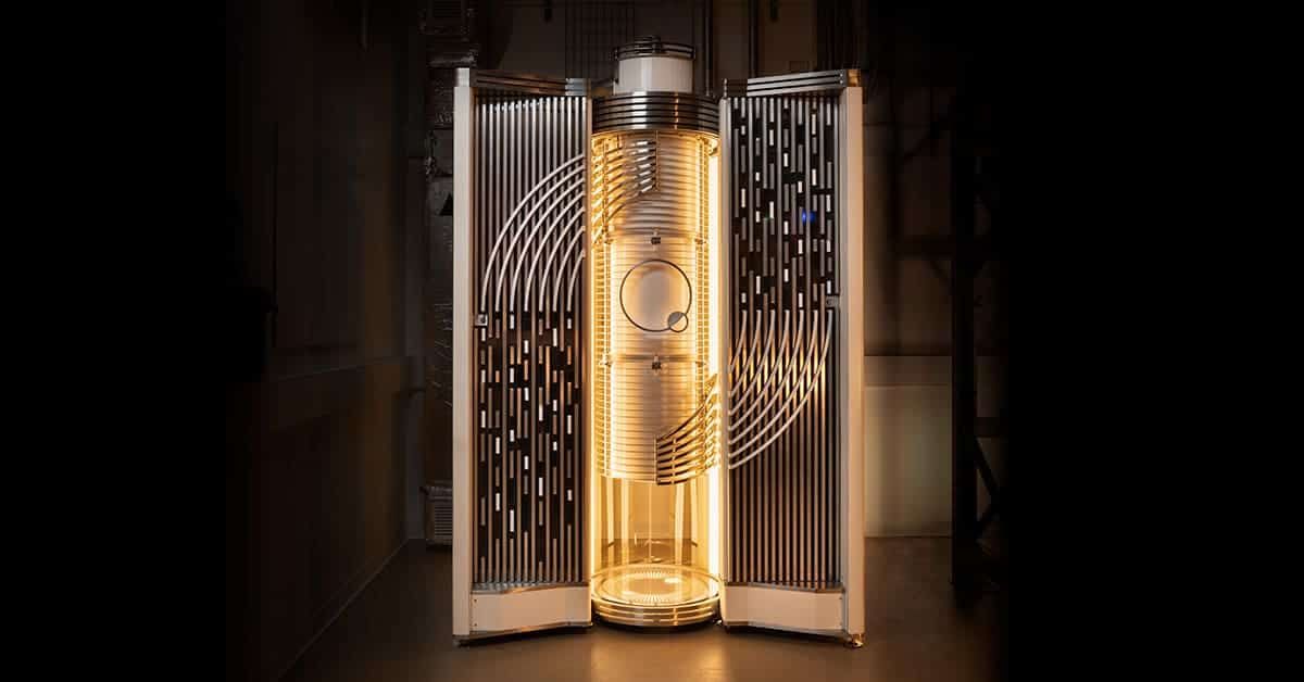
A British startup, Quantum Motion, has introduced what it describes as the world’s first silicon CMOS-based quantum computer —the same industrial foundation used to manufacture smartphone, laptop, and camera chips. The system, already installed at the National Quantum Computing Centre (NQCC), consolidates a dilution refrigerator and control electronics into three 19” racks, and combines a QPU (Quantum Processing Unit) with control software and interfaces compatible with environments like Qiskit or Cirq, offering a full-stack quantum computing platform.
Beyond the headlines, the story signals a shift in approach: moving from exotic, fab-specialized devices to 300 mm wafers and standard CMOS processing, with spin qubits (information encoded in the spin of an electron) integrated into a “tile” design—a modular, scalable framework intended for replication.
What exactly has been built
- Manufacturing technology: C MOS on natural silicon (300 mm wafer), the same “language” dominating classical electronics.
- Type of qubit: silicon spin qubits; the QPU integrates compute, readout, and control within a dense matrix that can be replicated via tiles/chiplets.
- System stacking: QPU + UI + control software (“industry-standard” layer translating algorithms into physical pulses), plus cryogenic electronics and dilution refrigerators to reach required temperatures.
- Physical footprint: ≈ 3 racks of 19”, including cooling and control (a surprisingly compact form factor for an operational quantum system).
The tile-based architecture condenses critical functions into repeatable blocks, enabling future QPUs to scale by increasing qubits through replication without system reengineering. The company envisions, in the medium term, scaling to millions of qubits, a goal still distant for the industry but aligned with the strategy of manufacturing quantum devices with CMOS tools.
Why silicon really matters
Most quantum roadmaps face two major hurdles: manufacturing large numbers of qubits with uniform quality and operating them with scalable electronics. CMOS silicon offers:
- Existing industrial supply chain: mature fabs, known standards, and performance. No need to build an industry from scratch.
- High-density integration: possibility of bringing control and readout close to the qubits, reducing cables and surfaces at cryogenic temperatures.
- Cost and repeatability: large production batches, statistical verification, and economies of scale currently unavailable in other quantum technologies.
The downside remains: spin qubits are fragile, requiring ultra-low temperatures (dilution refrigerators at millikelvin), and extremely precise pulsed control. But when they work well, they speak the language of modern manufacturing.
State of the art and precision context
The Quantum Motion system builds on previous results from its collaboration with University College London (UCL): achieving 98% fidelity on two-qubit gates (the basic entangling operation) in natural silicon on 300 mm, a competitive figure for the technology. This platform has been deployed at the NQCC within the Quantum Computing Testbed Programme, which explores seven prototypes with different technologies.
It’s important to differentiate: raw qubit counts (“Condor” from IBM with 1,121 qubits; Atom Computing with 1,180 neutral atoms) do not equate to useful qubits. Fidelity and connectivity determine whether error correction and practical circuits can be executed. The message here isn’t “more qubits than anyone,” but rather “CMOS-fabricated qubits” with fidelities aspiring to enter the realm of fault-tolerant systems.
Scaling promise: tiles today, millions of qubits tomorrow
The QPU unifies compute, readout, and control within a replicable matrix. In theory, simply “printing” more tiles can:
- Increase qubit count per chip (and wafer).
- Simplify signal routing and reduce cryogenic cabling.
- Enhance density and thermal stability by integrating more functions near the qubits.
Practically, progress depends on SiQEC (silicon-based quantum error correction project) and fault-tolerant architectures that multiply the number of physical qubits to build a few reliable logical qubits. These advances will be measured in error rates, QEC cycles, and overheads.
What sets this approach apart from other quantum methods
- Superconductors (transmons): powerful ecosystem (IBM, Google), high fidelities, but bulky cryogenic wiring and non-CMOS fabrication.
- Trapped ions: leading fidelities and modular scaling with traps and photonic links; electronics and fabrication differ from standard CMOS.
- Neutral atoms/photonic systems: great potential in entanglement and certain gates; with proprietary factories and supply chains.
- Silicon spin qubits (Quantum Motion): lower industrial barrier if well integrated into CMOS, with promise of density per tile and embedded control. The challenge: achieving sustained fidelities and interconnection at scale.
No “winner” yet: each approach involves trade-offs among fidelity, scalability, control, and ecosystem.
Industry implications (and for data centers)
- Form factor: about 3 racks (with fridge and control) —different from a typical cable-laden lab. For operators, this suggests more integrated solutions if cryogenic cooling and electronics standardize.
- Supply chain: if the front end is manufactured in 300 mm CMOS fabs, availability and cost could improve over exotic-process-dependent technologies.
- Control/readout: integrating RF/analog and multiplexing near the qubits is crucial to scaling up qubits without collapsing into hundreds or thousands of cryogenic lines.
- Software: compatibility with Qiskit/Cirq and industrial stacks reduces friction for benchmarking and hybrid workflows (classical + quantum).
- Roadmap: the metric isn’t just the standalone qubit, but demonstrations of QEC, surface codes, or equivalents, relying on logical qubits with meaningful lifetime.
Reasonable cautions
- Cooling: although the form factor resembles a rack, a dilution refrigerator remains necessary; operation is not trivial or comparable to a classic server.
- Fidelity and noise: 98% on two-qubit gates is not enough for efficient QEC; industry targets >99.9% for stability and reliability.
- Scaling vs. control: replicating tiles is necessary but not sufficient; inter-tile interconnects, clock/slash pulse distribution, and metrology are critical challenges.
- Timelines: “commercial quantum computers within the decade” is ambitious; expect iterations and intermediate milestones (specialized quantum accelerators, cloud services with time-sharing, etc.).
What to watch going forward
- Open benchmarks (Randomized Benchmarking, cross-entropy, reference circuits) on this platform, not extrapolated.
- End-to-end QEC demonstrations on silicon CMOS.
- Ecosystem: fab partners, cryogenic packaging, control platforms, material suppliers.
- Software compatibility: runtimes and compilers capable of translating algorithms without tricks into pulses with controlled latency and jitter.
- Repeatability: batches of 300 mm wafers with yields and variability measured; here lies the promise (or the risk) of “silicon-based quantum”.
Conclusion
Quantum Motion’s announcement doesn’t close debates, but it opens an exciting path: manufacturing quantum devices with silicon techniques. If spin qubits demonstrate improving fidelities, if CMOS integration reduces wiring, and if a tile can be reliably replicated, scalability —the quantum field’s Achilles’ heel— could lean on the world’s most mature manufacturing ecosystem. The remaining challenges are to demonstrate error correction at scale and sustainable logical qubits; until then, caution is advised. But the message is clear: quantum wants to speak CMOS, and the first prototype, in three racks, is already underway.
via: quantum motion