The race for artificial intelligence encounters a physical limit: heat. Each new generation of GPUs and AI accelerators increases power density and, with it, the temperature that data centers must dissipate. Microsoft claims to have reached a milestone with an “in-chip” microfluidic cooling system that, in laboratory tests, removed heat up to three times better than current cold plates. The method brings the coolant inside the silicon itself, where thermal generation is concentrated, through microchannels etched into the rear side of the chip and an AI-guided flow distribution targeting hotspots.
The company tested the system on a server running core services for a Microsoft Teams meeting simulation. According to its engineers, besides increasing the thermal ceiling, the technique reduced the maximum temperature rise by up to 65% within a GPU (a figure that, they note, will vary depending on chip type and configuration).
How it works: from “cooling on top” to “cooling inside”
Cold plates, now ubiquitous in high-density deployments, support a liquid circuit over the chip’s encapsulation. Between the heat source (the die) and the liquid, several layers—TIMs, spreaders, substrates—dampen the thermal exchange. The microfluidic approach eliminates intermediaries: etches microchannels—about the thickness of a human hair—directly into the silicon and circulates coolant through these channels. This shortens the thermal path, reduces losses, and allows operation with less cold refrigerant to extract the same (or greater) amount of heat, benefiting energy efficiency and operational costs.
The architecture is complex. The channels need to be deep enough to move flow without obstruction but not so deep as to weaken the die and compromise its integrity. Additionally, the final package requires absolute sealing, material compatibility with the fluid, new etching methods, and a manufacturing process that incorporates these additional steps without breaking industrial yields. Microsoft’s Cloud Operations and Innovation team reports iterating on four designs over the past year to balance these variables.
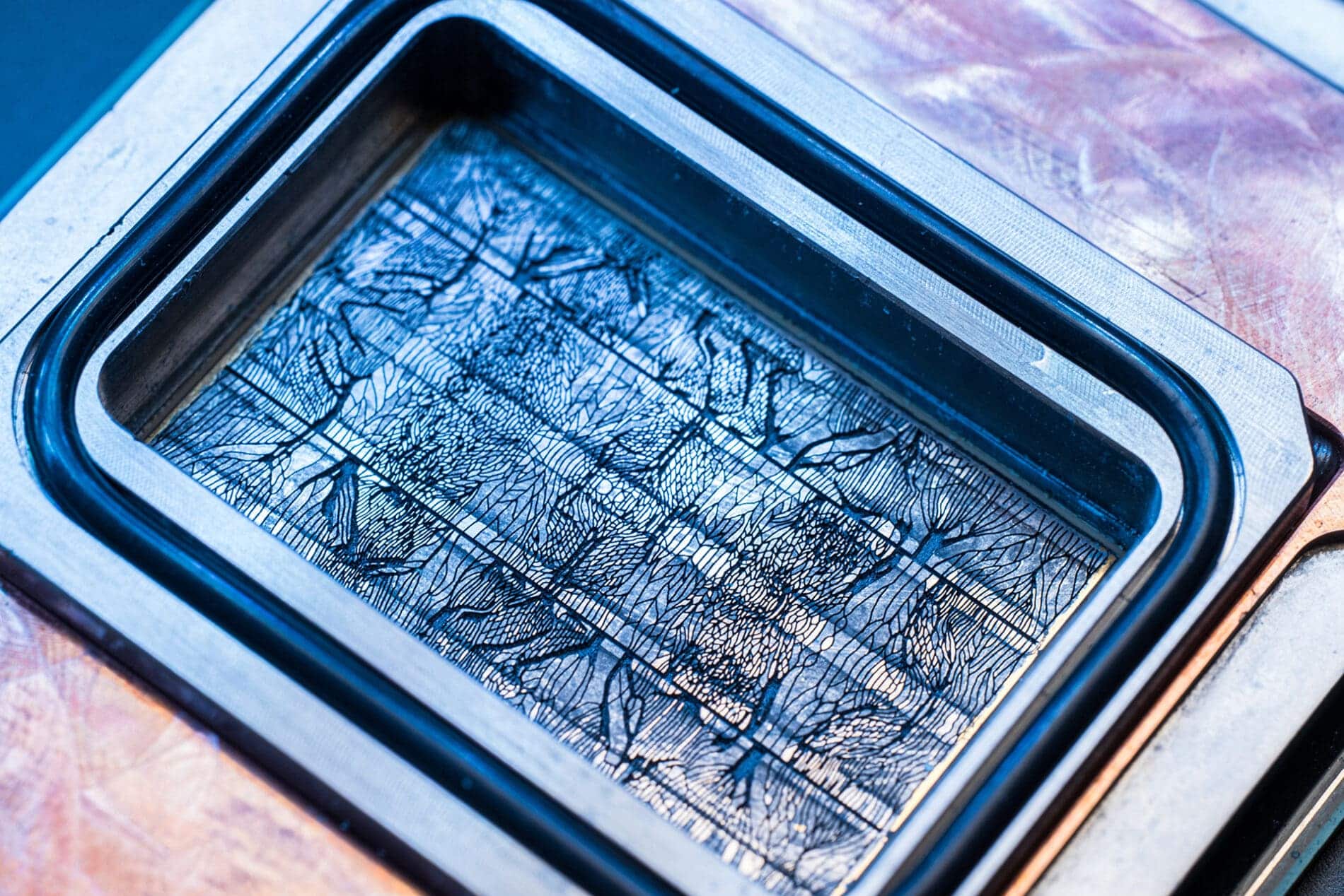
AI inspired by leaves: bioinspired microchannels
The company partnered with Swiss startup Corintis to optimize the microchannel geometry with a biomimetic design: instead of orthogonal grids, a venation-like branching—akin to a leaf or wing—distributes flow more efficiently to hotspots. The system complements this pattern with an AI model that identifies unique thermal signatures of each chip and guides flow where needed based on workload, reducing bottlenecks that uniform channels cannot resolve.
This idea echoes a systems engineering intuition: not all parts of a chip heat up equally or simultaneously. In real-world scenarios—ranging from transcoding to an attention kernel—the thermal footprint varies. With adaptive cooling, the thermal budget for peaks increases, providing a margin for peak performance without compromising reliability.
Why now? The cold plate ceiling
Microsoft warns that in five years, continued over-reliance on cold plates will hit a ceiling for power per chip and rack. The reason is twofold. First, each layer between liquid and die reduces thermal coefficient. Second, the evolution of GPUs with more HBM, cores, and higher frequency causes the heat flux per millimeter to grow faster than encapsulated cooling solutions can remove it.
Microfluidic cooling brings the fluid closer to the source, raising the thermal ceiling and opening the door to new architectures: from denser racks (more servers per meter) to stacked 3D chips with microfluidic “pillars” circulating fluid between layers—an image engineers compare to multilevel parking supports with coolant flowing around.
Beyond the thermometer: density, PUE, and safe overclocking
The company associates three systemic effects with this technique:
- Compute density: By raising the thermal ceiling, servers can be closer together without entering temperature zones that compromise reliability. Less distance means lower latency between nodes and more performance per rack.
- Energy efficiency (PUE): If the coolant does not need to be as cold to perform the same work, less energy is used to cool the liquid. This saves electricity and, according to Microsoft, reduces strain on the local network.
- Operational flexibility: For services with peaks—like Teams, which concentrates connections at the start of each band—being able to temporarily boost performance (controlled overclocking) without crossing thermal thresholds protects the SLA without over-dimensioning idle capacity.
A puzzle of materials, processes, and reliability
Engineering enthusiasm coexists with manual challenges that still need solving to move from the lab to the manufacturer and then to the data center:
- Microfabrication: integrating channel etching into each foundry process line with tight tolerances and industrial yields.
- Package mechanics: ensuring seal integrity, material compatibility with the fluid, resistance to thermal cycles and vibration, and maintenance without degrading the chip.
- Quality and control: detecting microcracks or clogging in microscopic channels using non-destructive methods and reasonably reparable.
- Standards: defining interfaces and protocols to prevent microfluidic solutions from becoming closed ecosystems with prohibitively high operating costs.
Microsoft states that its next phase focuses on reliability (reliability) and industrializing the method with manufacturing partners to include it in future Cobalt and Maia chips, as well as exploring its generalization with third parties in Azure.
The context: record investment and a full-stack approach
The microfluidic push fits into a broader strategy: tuning every layer of the cloud—from silicon to the data hall—to maximize performance and contain consumption. The company plans to spend over $30 billion in capex this quarter, an amount aligned with expanding capacity and modernizing infrastructure with own chips optimized for customer workloads.
However, chips are just one piece of a complex system. Tables, racks, networks, fiber, and orchestration software must all move in concert for thermal gains to translate into speed, stability, and competitive unit costs.
What does this mean for the industry?
If in-chip cooling becomes standardized, its impact will surpass a single provider or hyperscaler. Unlocking the thermal ceiling opens space for more cores, more memory, higher bandwidth, and stacked chips, leading to smaller yet more powerful data centers. It could also increase the reuse of higher-quality residual heat (at higher, controlled temperatures), useful for heat networks or nearby industrial processes.
The flip side: manufacturing complexity and cost, maintenance, and repair. Sending liquid inside the die makes each failure more costly; balancing thermal benefits with economic viability will be essential. Industry history suggests a likely path: initially in premium and large-scale services, then cost reductions and wider adoption.
FAQs
How does microfluidic cooling differ from cold plates?
Cold plates extract heat from above the encapsulation of the chip; in-chip microfluidic etches channels into the silicon and circulates coolant inside the chip. This shortens the thermal distance and improves heat extraction, enabling operation with less cold refrigerant and potentially enhancing the data center’s PUE.
What real improvements has Microsoft measured?
In lab tests, it achieved up to three times better heat extraction compared to cold plates and reductions of 65% in the maximum temperature rise of a GPU (depending on workload and design). The scale-up to production will depend on chip type, fluid, package, and process.
Can it enable stacked 3D chips?
Yes, by bringing coolant close to the points of consumption, microfluidics opens pathways for interlayer cooling in 3D architectures, with “pillars” (cylindrical pins) around which fluid flows.
When might it see production?
The technology is in advanced prototype and reliability testing. Next steps involve industrialization with foundries and partners, and integrating into future chips and data centers. The timeline depends on manufacturing fit and ecosystem maturity.
via: news.microsoft