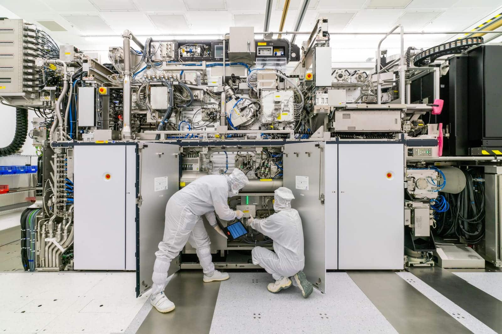
The future of the semiconductor industry is closely linked to the ability to shrink transistors even further onto silicon wafers. In this arena, ASML, the Dutch company dominating the lithography market, once again hits a milestone with its TWINSCAN EXE:5200B system, the second generation of High-NA EUV lithography equipment with high numerical aperture (0.55 NA).
This new scanner represents a leap forward from conventional EUV systems (0.33 NA) and promises transistor densities up to 2.9 times higher, reducing manufacturing process complexity and increasing factory output.
What is High-NA EUV Lithography?
Lithography is the core of microchip fabrication: it involves projecting light onto a silicon wafer coated with photosensitive material to print nanometer-scale patterns.
- Current EUV systems operate with 13.5 nm wavelength light and an NA of 0.33.
- With High-NA (0.55), engineers achieve greater image contrast and resolutions up to 8 nm, enabling the printing of features 1.7 times smaller in a single exposure.
The EXE:5200B combines this precision with improvements in the EUV light source — based on plasmas generated by vaporizing tin droplets with lasers — and with advanced optics developed alongside ZEISS SMT, optimized to reduce aberrations.
Why It Matters: Density and Productivity
The new ASML system offers:
- 40% more image contrast compared to current NXE systems.
- 8 nm resolution, crucial for future nodes of 14A and beyond.
- Higher productivity, with the ability to expose wafers faster thanks to a more powerful EUV source.
This translates to more chips per wafer, reduced process complexity, and higher mass production efficiency.
From Theory to Production
The history of EUV spans decades: from early prototypes in the 80s and 90s to the launch of NXE:3300 in 2013. Major adoption began in 2016, when the technology started being utilized at significant volumes.
The transition to High-NA now marks a second revolution. The first EXE system was delivered in December 2023, with volume production anticipated for 2025–2026.
The Cost of the Future: A Multibillion-Dollar Investment
The advancement comes with controversy. The EXE:5200B costs around $380 million per unit, compared to $235 million for conventional EUV equipment. This cost increase explains why manufacturers like Intel have already warned that their future nodes (14A) will be more expensive than current ones (18A), despite offering significant gains in efficiency and density.
The challenge is twofold: justify the investment for foundries’ customers and demonstrate that productivity will offset the initial costs.
ASML’s View: Hardware and Software as One
While many see ASML purely as a hardware company, the firm insists its systems are a hybrid of optics, precision mechanics, and advanced software.
- The hardware is the “Batman,” responsible for the physical components.
- The software is the “Robin,” essential for correcting imperfections, managing aberrations, and enabling the machines to reach their physical limits.
Without these combined innovations, it would be impossible to produce chips with billions of transistors on a hand-sized wafer.
Strategic and Global Impact
The advent of High-NA is not just a technological leap; it’s a strategic move to redistribute power within the industry.
- For Intel, it’s the key to their 14A node and their foundry strategy (IFS).
- For TSMC and Samsung, it’s a decision point—whether to adopt High-NA soon or to continue with conventional EUV to keep costs lower.
- For Europe, ASML’s success is vital: it’s the only region controlling this critical technology amidst geopolitical tensions and digital sovereignty concerns.
Frequently Asked Questions (FAQ) about EUV High-NA and the EXE:5200B
What is the difference between conventional EUV and High-NA EUV?
Conventional EUV (0.33 NA) offers resolutions up to 13 nm. High-NA (0.55 NA) improves contrast and enables resolutions of 8 nm, with densities 2.9 times higher.
Why is an EXE:5200B scanner so expensive?
Because it integrates ZEISS’s atomic-level precision optics, laser-based EUV sources with high power, and mechanical systems capable of moving wafers at extreme speeds with nanometric accuracy. Each unit costs approximately $380 million.
Which manufacturers will use High-NA EUV?
Intel has confirmed usage in the 14A node. TSMC and Samsung are still evaluating whether to adopt it soon or wait.
When will it be available for mass production?
The first EXE units have already been delivered (since 2023), and volume production is expected between 2025 and 2026.