The Japanese Seiki Semiconductor Co., Ltd. (Seiki Semi), with a strong presence in Taiwan, introduced at SEMICON Taiwan 2025 its new 82CWW series, a dual-mode hybrid bonding system that promises to mark a turning point in advanced semiconductor packaging.
This announcement reinforces the company’s strategy of localizing equipment manufacturing in Taiwan, a key country within the global supply chain, at a time when demand for AI (artificial intelligence), high-performance computing (HPC), and automotive technologies is driving heterogeneous integration and 3D stacking.
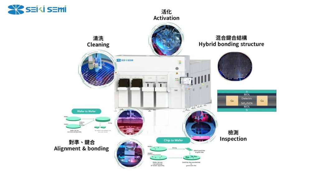
A system designed for precision and scalability
The 82CWW Series enables both chip-to-wafer (C2W) and wafer-to-wafer (W2W) bonding, making it a versatile tool for R&D projects and large-scale manufacturing.
Its capabilities include:
- Compatibility with 8 and 12-inch wafers.
- Handling ultrathin wafers up to 35 μm thick.
- Chips ranging from 0.5 × 0.5 mm to 50 × 50 mm.
- Bonding accuracy of ±100 nm.
- Output of up to 1,000 chips per hour.
Additionally, the system features advanced characteristics such as dual alignment (coaxial and infrared), interchangeable modules for quick reconfiguration, and real-time deviation compensation through high-speed detection and feedback algorithms. All these features are designed to maximize precision, reduce downtime, and ensure consistent performance.
Voices of the pioneers: Tadatomo Suga’s session
As part of the SEMICON Taiwan 2025 program, Seiki Semi hosted a prominent session led by Tadatomo Suga from the University of Tokyo, recognized as one of the pioneers of hybrid bonding technology.
His presentation, titled “Advanced Hybrid Bonding Technologies and Applications”, addressed how advanced packaging and 3D integration are helping overcome bottlenecks in systems for AI and HPC. Suga emphasized the importance of cross-sector collaboration to keep pace with industry-driven innovation.
Hybrid bonding, a strategic technology
Hybrid bonding is gaining prominence as a key technology in heterogeneous integration and 3D circuit stacking. Its adoption is considered critical for sustaining Moore’s Law through combining different chip types—such as memory, CMOS image sensors, micro-LEDs, or silicon photonics—within a single system.
In this context, Seiki Semi’s commitment to strengthening its R&D in Taiwan underscores the island’s strategic role in the global semiconductor supply chain, a sector where innovation in packaging has become as critical a differentiator as wafer fabrication processes.
A trusted partner for the global industry
With over 20 years of experience, Seiki Semi has developed hybrid bonding equipment and processes used in memory, next-generation displays, and semiconductors for communications and automotive applications. Besides supplying equipment, the company offers OEM bonding services for manufacturers, solidifying its position as a comprehensive partner within the advanced packaging ecosystem.
📌 Frequently Asked Questions (FAQ)
1. What is hybrid bonding in semiconductors?
It’s a technique combining mechanical and electrical bonding at the chip or wafer level, enabling high-precision, reliable integration of different components within 3D architectures.
2. What are Seiki Semi’s technology applications?
Its systems are used in manufacturing memory chips, CMOS sensors, micro-LEDs, silicon photonics, and heterogeneous wafer-level integration systems.
3. Why is Taiwan strategic for Seiki Semi’s strategy?
Because Taiwan hosts a significant portion of global semiconductor manufacturing and is a central innovation hub for packaging, facilitating collaboration, proximity to customers, and supply chain resilience.
4. What advantages does the new 82CWW system offer over other solutions?
Its dual bonding modes (C2W and W2W), high precision (±100 nm), and capacity to produce 1,000 chips per hour, along with alignment and real-time compensation tools, make it a highly scalable solution for both R&D and manufacturing.
via: semicontaiwan