China has just made a significant move in the race for semiconductor technological sovereignty. During the 2025 Integrated Circuit Innovation and Development Conference held in Wuxi (Jiangsu Province), the launch of the country’s first national project capable of producing advanced resins and photoresists for EUV lithography was announced. This development, focused on MOR (Metal Oxide Resist) technology, makes China the first country outside of ASML and its partners to master a critical component of the ecosystem for 5-nanometer (and smaller) chips.
The context: EUV lithography, the technological frontier
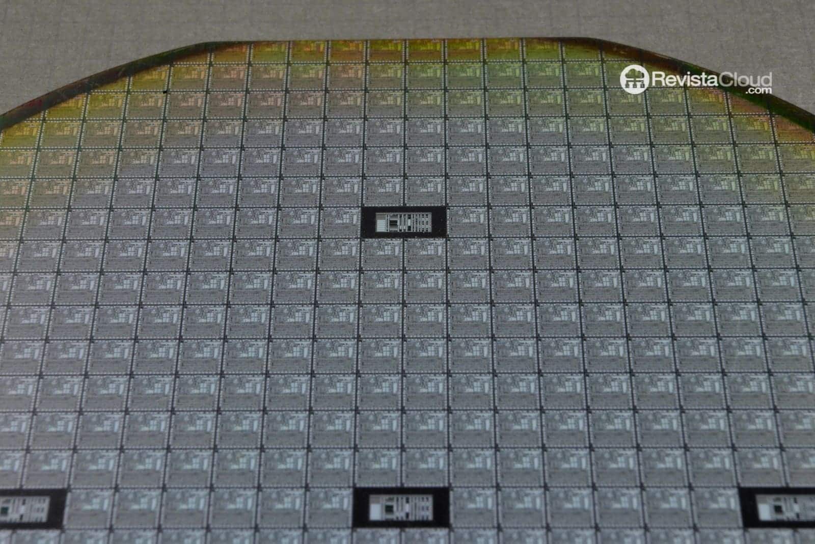
EUV (Extreme Ultraviolet Lithography) is the process used to etch the finest patterns on silicon wafers, enabling the manufacture of chips with transistors at just a few nanometers in size. Until now, this technology has been nearly exclusively controlled by the Dutch company ASML, which develops the most advanced exposure machines, and by a handful of Japanese and US suppliers specialized in materials.
While the machines — such as ASML’s EUV Twinscan — often steal the spotlight, photoresists are just as essential: without them, it’s impossible to leverage the 13.5 nm wavelength EUV light to print structures with atomic-scale precision.
Transition to MOR: beyond traditional CARs
Current deep ultraviolet (DUV) photoresists are based on CAR (Chemical Amplified Resist) compounds. Although effective, these materials face resolution limitations necessary for nodes of 5 nm, 3 nm, or smaller.
The new development announced in Wuxi focuses on MOR (Metal Oxide Resist), metal oxide-based photoresists that offer:
- Higher resolution: reducing transistor gate distances.
- Lower defect rates: decreasing exposure errors.
- Greater stability: improved responses to EUV light and subsequent etching processes.
In this way, China aims not only to become self-sufficient in a strategic material but also to match the most advanced global solutions.
Two strategic projects in Wuxi
During the conference, two innovative initiatives were presented that outline the country’s roadmap for EUV materials:
- Pilot line for EUV MOR photoresists: the first national project with the capacity to control raw materials, formulation, and application of metal oxide photoresists.
- Pilot line for EUV resins with continuous flow synthesis: a unique Chinese project utilizing a stable polymerization process through advanced synthesis equipment.
Both projects, aligned with the semiconductor technological self-sufficiency strategy, aim to reduce reliance on imports and accelerate domestic manufacturing capabilities at cutting-edge nodes.
Impact on memory and advanced logic chips
The significance of new MOR photoresists extends beyond 5 nm and 3 nm logic chips. Their application is also expected in memory industries:
- DRAM: beginning to adopt EUV to reduce size and boost performance.
- NAND Flash: although not yet requiring EUV at scale, future high-density generations will inevitably do so.
This leap will help Chinese manufacturers narrow the technological gap with leaders like Samsung, SK Hynix, and TSMC.
The geopolitical challenge
The announcement comes amidst intense international pressure. The United States and allies have imposed restrictions on exporting advanced EUV equipment to China, aiming to limit its progress in cutting-edge semiconductors.
The local development of materials like MOR photoresists is a critical link to reduce dependency, though the largest hurdle remains exposure machines, where ASML maintains at least a decade-long lead.
Nevertheless, analysts suggest that controlling key materials can provide China with greater maneuvering room, as lithography involves a full chain of processes and highly specialized consumables beyond the machines themselves.
Looking to the future
The path ahead will be challenging. Mastering large-scale production of EUV MOR photoresists requires:
- Ensuring process stability at high volumes.
- Achieving extreme purities in chemical compounds.
- Coordinating with the global supply chain to certify compatibility with foundries.
Nevertheless, the Wuxi project signifies a turning point: for the first time, China positions itself in the arena of next-generation EUV materials, with a proposal aiming to compete with Japan and the US.
Conclusion
The launch of China’s first center dedicated to developing MOR EUV photoresists marks a milestone in the quest for technological sovereignty. While the country still depends on imported advanced lithography equipment, its focus on mastering critical materials is a strategic step that could reshape its role in the global semiconductor supply chain.
The industry’s future will hinge not only on machine advances but also on each country’s capacity to innovate in chemical materials that can continue shrinking transistor sizes. In this arena, China has just made its move.
FAQs (Frequently Asked Questions)
What is a MOR photoresist?
It is a type of EUV lithography photoprotector based on metal oxides (Metal Oxide Resist), offering higher resolution and fewer defects at 5 nm nodes and beyond, surpassing the limitations of traditional CAR photoresists.
Why is China’s production of EUV photoresists so important?
Because photoresists are critical inputs in manufacturing next-generation chips. Until now, China relied on foreign suppliers, mainly Japanese and US companies.
In which industries will this technology be used?
Besides 5 nm and 3 nm logic chips, it will be applied to DRAM memory and future high-density NAND Flash generations.
How does this advance influence the geopolitical landscape?
It reinforces China’s strategy of technological self-reliance amid export restrictions imposed by the US and EU. Although it still lags behind ASML in EUV machinery, controlling key materials grants greater autonomy.
via: Mydrivers