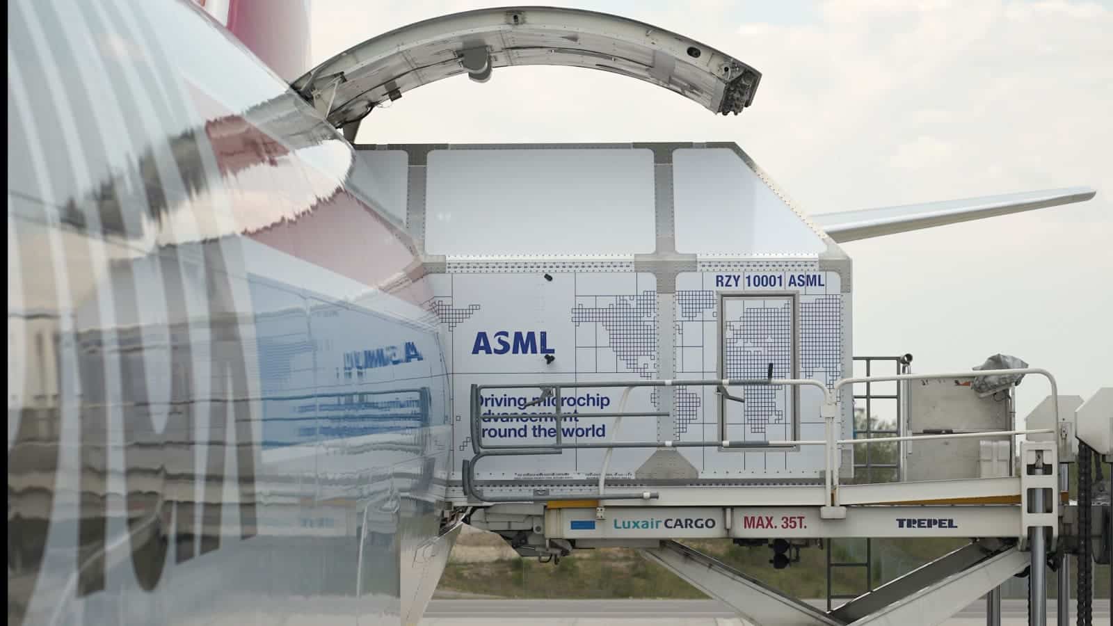
The Dutch ASML, a global leader in lithography equipment for semiconductor manufacturing, participated for the first time in SEMICON India 2025. This gesture confirms its strategic interest in one of the most promising markets of the next decade.
The company showcased its holistic lithography approach, an integrated method that combines advanced lithography systems, computational software, metrology, and inspection, aimed at helping chip manufacturers produce smaller, more powerful, and efficient semiconductors — while reducing manufacturing errors and enhancing performance.
A Growing Market: From $55 Billion to $100 Billion
India has been identified as one of the new hubs of the semiconductor industry. According to official projections, its market will surpass $55 billion by 2026 and reach $100 billion by 2030, driven by smartphone, automotive, 5G, and IoT demand, with strong government support through investments and incentives.
ASML believes its technologies can play a key role in this growth, providing new Indian factories with the tools needed to rapidly scale operations and stay competitive against established giants such as Taiwan, South Korea, and the United States.
ASML’s Holistic Lithography Strategy
During the event, ASML explained how their integrated approach allows for maximized process window and increased daily wafer output. Their strategy rests on three pillars:
- Advanced lithography systems: utilizing nanometer-precision light to print patterns on silicon wafers.
- Computational lithography software: implementing automated control loops and online adjustments to optimize performance.
- Metrology and inspection: enabling critical dimension measurements, alignment verification, and defect detection before mass production is affected.
The combination of these three areas provides a competitive edge for emerging fabs by reducing errors, improving efficiency, and ensuring scalability for future technologies.
India as a Strategic Partner
In his speech, Christophe Fouquet, President and CEO of ASML, emphasized the significance of this moment:
“India has shown remarkable progress in advancing its ambitions in the semiconductor industry, with investments, a solid talented workforce, and clear government support. We celebrate India’s vision because it strengthens the entire global industry. Through our first participation in SEMICON India, we hope to learn more about its ecosystem, establish new relationships, and prepare opportunities.”
This message reinforces ASML’s goal of positioning itself as a key technological partner in India, a country aiming to reduce reliance on imports and to become a pivotal player in the global chip supply chain.
Global Implications
ASML’s interest in India isn’t coincidental. The geopolitical pressures surrounding semiconductors — marked by restrictions on China, technological competition with the U.S., and concentrated production in Taiwan — have accelerated the search for new manufacturing hubs.
With its massive domestic market and a dedicated effort to attract foreign factories, India is emerging as a strategic alternative. For ASML, entering this ecosystem not only diversifies its customer base but also expands the influence of its EUV and DUV lithography technologies in a market ready to leap to the most advanced nodes.
Conclusion
The presence of ASML at SEMICON India 2025 marks a turning point in the company’s expansion strategy. More than a product showcase, it’s a declaration of intent: India is on the radar of industry giants, and ASML wants to be part of its industrial takeoff.
If India can solidify its semiconductor market, ASML’s lithography will be an indispensable component on its path toward the $100 billion projected for 2030.
Frequently Asked Questions (FAQ)
Why is ASML so important in the semiconductor industry?
Because it manufactures the world’s only EUV lithography machines, essential for producing cutting-edge chips in advanced nodes (3 nm, 2 nm, and beyond).
What does ASML’s holistic lithography mean?
It’s an approach that combines lithography, computational software, metrology, and inspection to optimize manufacturing processes and boost performance.
What opportunities does India open for ASML?
An emerging market with enormous projected growth. For ASML, this means expanding its influence in a new chip manufacturing hub.
How does this move impact global technological sovereignty?
It strengthens India as an alternative to Taiwan, South Korea, or China and diversifies the chip supply chain, reducing dependence on a few critical regions.
via: asml