A pilot project will give students at over 40 universities the opportunity to design and manufacture their own chips, bringing the semiconductor industry closer to academia.
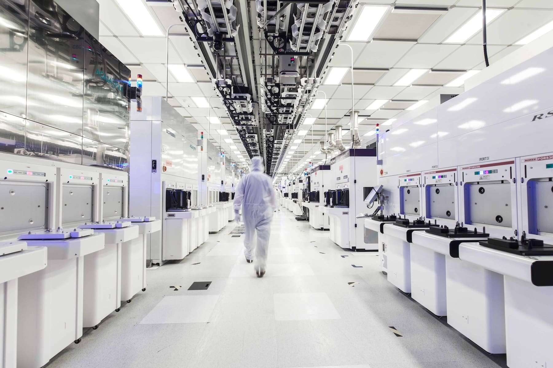
The shortage of skilled semiconductor talent is one of the industry’s biggest concerns worldwide. Aware of this, Synopsys — a leader in electronic design automation (EDA) software — and GlobalFoundries (GF) — one of the largest chip manufacturers in the world — have announced a strategic partnership to launch a pilot educational program that will allow students to experience the full cycle of chip design and manufacturing, from initial idea to tapeout and functional silicon return.
The project is already being tested at more than 40 universities around the world and aims to expand in the coming years. The initiative combines access to Synopsys design solutions with GF’s manufacturing capacity through their GlobalShuttle Multi-Project Wafer (MPW) program, which consolidates designs from different institutions onto a single wafer to reduce prototyping costs.
A unique hands-on experience
The educational plan is designed to break down economic and technical barriers that usually hinder universities from experimenting with real silicon. Students will work with professional cloud-based tools from Synopsys, and after completing the design, GF will handle the fabrication of the chips. Once back in the classroom, students can test and validate their chips, closing a learning cycle that until now was reserved for leading companies or research centers.
“It’s not just about teaching chip design but about preparing the next generation of engineers who will shape the future of the industry,” said Patrick Haspel, executive director of Synopsys’s academic program (SARA).
Meanwhile, Bika Carter, Director of External R&D at GlobalFoundries, emphasized that “giving students the chance to bring their ideas from concept to silicon in a real environment strengthens semiconductor design education and helps build the talent pool that the industry desperately needs.”
How the program works
- Stage 1: Training teachers and students on how to use Synopsys’s EDA tools.
- Stage 2: Collaborative chip design in class, guided by professionals and academic materials.
- Stage 3: Submitting designs through GF’s GlobalShuttle MPW for manufacturing.
- Stage 4: Receiving the fabricated chips back for testing and validation in the next semester.
Besides providing practical experience, the program also aims to bring university research closer to industry needs, aligning with GF’s roadmap in areas like RF, silicon photonics, sensors, quantum computing, and communications.
Educational and strategic value
This collaboration is supported by Synopsys’s SARA academic program, which provides software, training, and curricular content. On GF’s side, it is part of their University Partnership Program, which already collaborates with over 80 universities and 600 students on innovation projects.
This pilot project has a dual impact:
- Educational: Expands opportunities for practical learning, especially critical in a context where demand for microelectronics engineers far exceeds supply.
- Strategic: Contributes to strengthening technological sovereignty and reducing dependence on certain production hubs, diversifying both talent and innovation capacity.
In Haspel’s words, “it’s a game-changer that democratizes access to chip design and manufacturing.”
Frequently Asked Questions
What is a tapeout in chip design?
The “tapeout” is the final phase of chip design when the layout is sent to the factory for silicon production.
What advantages does the program offer universities?
It eliminates prototyping cost barriers, allows students to work with professional tools, and provides real chips for classroom validation.
Which universities are participating in the pilot?
Over 40 institutions worldwide, though the full list has not been published. More institutions are expected to join in the coming years.
What impact could this program have on the semiconductor industry?
It could help reduce talent gaps, train professionals with practical experience, and accelerate innovation in critical areas like photonics, sensors, and quantum computing.
via: news.synopsys